MC74HC367 データシートの表示(PDF) - Motorola => Freescale
部品番号
コンポーネント説明
一致するリスト
MC74HC367
Motorola => Freescale

MC74HC367 Datasheet PDF : 5 Pages
| |||
MOTOROLA
SEMICONDUCTOR TECHNICAL DATA
Hex 3-State Noninverting
Buffer with Separate 2-Bit
and 4-Bit Sections
High–Performance Silicon–Gate CMOS
The MC54/74HC367 is identical in pinout to the LS367. The device inputs
are compatible with standard CMOS outputs; with pullup resistors, they are
compatible with LSTTL outputs.
This device is arranged into 2–bit and 4–bit sections, each having its own
active–low Output Enable. When either of the enables is high, the affected
buffer outputs are placed into high–impedance states. The HC367 has
noninverting outputs.
• Output Drive Capability: 15 LSTTL Loads
• Outputs Directly Interface to CMOS, NMOS, and TTL
• Operating Voltage Range: 2 to 6 V
• Low Input Current: 1 µA
• High Noise Immunity Characteristic of CMOS Devices
• In Compliance with the Requirements Defined by JEDEC Standard
No. 7A
• Chip Complexity: 92 FETs or 23 Equivalent Gates
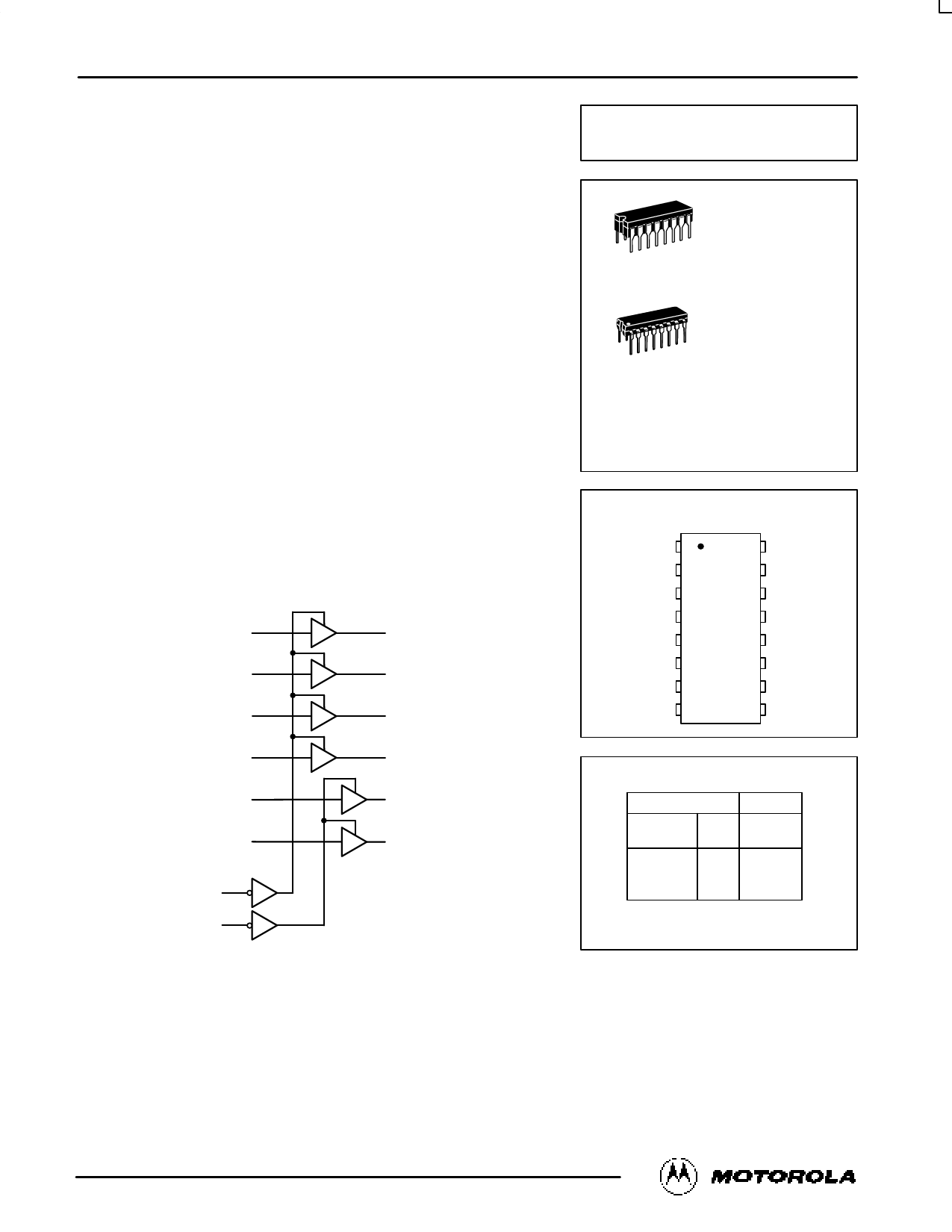
LOGIC DIAGRAM
A0 2
A1 4
A2 6
A3 10
A4 12
A5 14
3 Y0
5 Y1
7 Y2
9 Y3
11 Y4
13 Y5
OUTPUT ENABLE 1 1
OUTPUT ENABLE 2 15
PIN 16 = VCC
PIN 8 = GND
MC54/74HC367
16
1
J SUFFIX
CERAMIC PACKAGE
CASE 620–10
16
1
N SUFFIX
PLASTIC PACKAGE
CASE 648–08
ORDERING INFORMATION
MC54HCXXXJ
MC74HCXXXN
Ceramic
Plastic
PIN ASSIGNMENT
OUTPUT
ENABLE 1
1
A0 2
Y0 3
16 VCC
15
OUTPUT
ENABLE 2
14 A5
A1 4
13 Y5
Y1 5
12 A4
A2 6
11 Y4
Y2 7
10 A3
GND 8
9 Y3
FUNCTION TABLE
Inputs
Enable 1,
Enable 2 A
Output
Y
L
L
L
L
H
H
H
X
Z
X = don’t care
Z = high impedance
10/95
© Motorola, Inc. 1995
1
REV 6
Share Link: