CY23S08(2004) データシートの表示(PDF) - Cypress Semiconductor
部品番号
コンポーネント説明
一致するリスト
CY23S08 Datasheet PDF : 8 Pages
| |||
PRELIMINARY
CY23S08
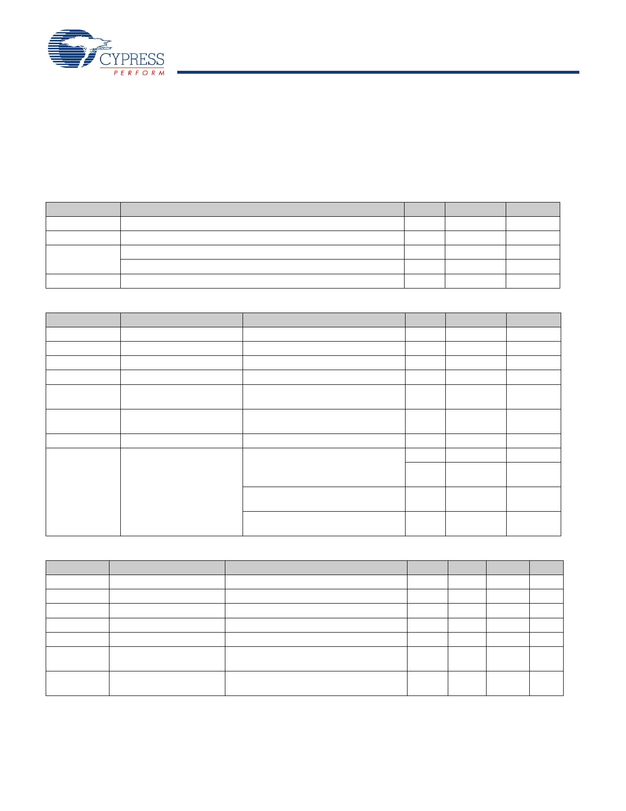
Switching Characteristics for CY23S08SC-XX Commercial Temperature Devices (continued)[8]
Parameter
t3
t4
t4
t4
t5
Name
Test Conditions
Rise Time[7] (–1H, -2H) Measured between 0.8V and 2.0V, 30-pF load
Fall Time[7] (–1, –2, –3, –4) Measured between 0.8V and 2.0V, 30-pF load
Fall Time[7] (–1, –2, –3, –4) Measured between 0.8V and 2.0V, 15-pF load
Fall Time[7] (–1H, 2H)
Measured between 0.8V and 2.0V, 30-pF load
Output to Output Skew on All outputs equally loaded
same Bank (–1)[7]
Output to Output Skew on All outputs equally loaded
same Bank
(–1H,–2,–2H,–3)[7]
Output to Output Skew on All outputs equally loaded
same Bank (–4)[7]
Output to Output Skew
(–1H, -2H)
All outputs equally loaded
Output Bank A to Output All outputs equally loaded
Bank B Skew (–1,–2, –3)
Output Bank A to Output All outputs equally loaded
Bank B Skew (–4)
Output Bank A to Output All outputs equally loaded
Bank B Skew (–1H)
t6
t7
t8
tJ
tJ
tLOCK
Delay, REF Rising Edge to
FBK Rising Edge[7]
Measured at VDD/2
Device to Device Skew[7] Measured at VDD/2 on the FBK pins of devic-
es
Output Slew Rate[7]
Measured between 0.8V and 2.0V on –1H,
–2H device using Test Circuit #2
Cycle to Cycle Jitter[7]
(–1, –1H)
Measured at 66.67 MHz, loaded outputs, 15,
30-pF loads: 133 MHz, 15-pF load
Cycle to Cycle Jitter[7]
(–2)
Measured at 66.67 MHz, loaded outputs,
15-pF load
Cycle to Cycle Jitter[7]
(–2)
Measured at 66.67 MHz, loaded outputs,
30-pF load
Cycle to Cycle Jitter[7]
(–3,–4)
Measured at 66.67 MHz, loaded outputs
15,30-pF loads
PLL Lock Time[7]
Stable power supply, valid clocks presented
on REF and FBK pins
Min.
–250
1
Typ.
0
0
Max.
1.50
2.20
1.50
1.25
200
150
100
200
300
215
250
+275
700
125
300
400
200
1.0
Unit
ns
ns
ns
ns
ps
ps
ps
ps
ps
ps
ps
ps
ps
V/ns
ps
ps
ps
ps
ms
Switching Waveforms
Duty Cycle Timing
1.4V
t1
t2
1.4V
1.4V
All Outputs Rise/Fall Time
2.0V
OUTPUT 0.8V
t3
2.0V
0.8V
t4
3.3V
0V
Document #: 38-07265 Rev. *D
Page 4 of 8
Share Link: 