TPC8102 データシートの表示(PDF) - Toshiba
部品番号
コンポーネント説明
一致するリスト
TPC8102 Datasheet PDF : 7 Pages
| |||
Electrical Characteristics (Ta = 25°C)
Characteristics
Gate leakage current
Drain cut−off current
Drain −source breakdown
voltage
Gate threshold voltage
Drain−source ON resistance
Forward transfer admittance
Input capacitance
Reverse transfer capacitance
Output capacitance
Rise time
Symbol
IGSS
IDSS
Test Condition
VGS = ±16 V, VDS = 0 V
VDS = −30 V, VGS = 0 V
V (BR) DSS ID = −10 mA, VGS = 0 V
Vth
RDS (ON)
RDS (ON)
|Yfs|
Ciss
Crss
Coss
VDS = −10 V, ID = −1 mA
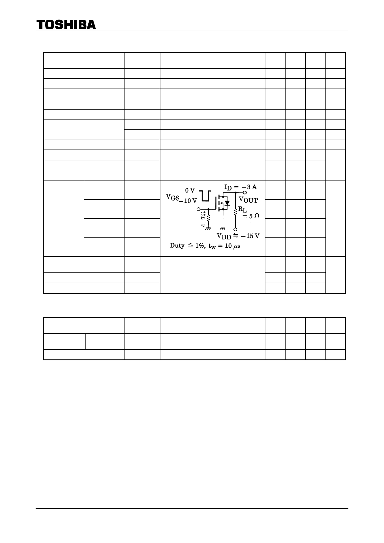
VGS = −4 V, ID = −3 A
VGS = −10 V, ID = −3 A
VDS = −10 V, ID = −3 A
VDS = −10 V, VGS = 0 V, f = 1 MHz
tr
Turn−on time
ton
Switching time
Fall time
tf
Turn−off time
Total gate charge (Gate−source
plus gate−drain)
Gate−source charge
Gate−drain (“miller”) charge
toff
Qg
Qgs
VDD ≈ −24 V, VGS = −10 V, ID = −6 A
Qgd
Source−Drain Ratings and Characteristics (Ta = 25°C)
Characteristics
Drain reverse
current
Pulse (Note 1)
Forward voltage (diode)
Symbol
IDRP
VDSF
Test Condition
—
IDR = −6 A, VGS = 0 V
TPC8102
Min Typ. Max Unit
—
—
±10
µA
—
—
−10
µA
−30
—
—
V
−0.8
— −2.0
V
—
56
70
mΩ
—
34
40
mΩ
4.5
9
—
S
— 1380 —
—
220
—
pF
—
560
—
—
12
—
—
20
—
ns
—
22
—
—
90
—
—
43
—
—
30
—
nC
—
13
—
Min Typ. Max Unit
—
—
−24
A
—
—
1.2
V
3
2002-01-18
Share Link: 