ISL8499 データシートの表示(PDF) - Renesas Electronics
部品番号
コンポーネント説明
一致するリスト
ISL8499
Renesas Electronics

ISL8499 Datasheet PDF : 14 Pages
| |||
ISL8499
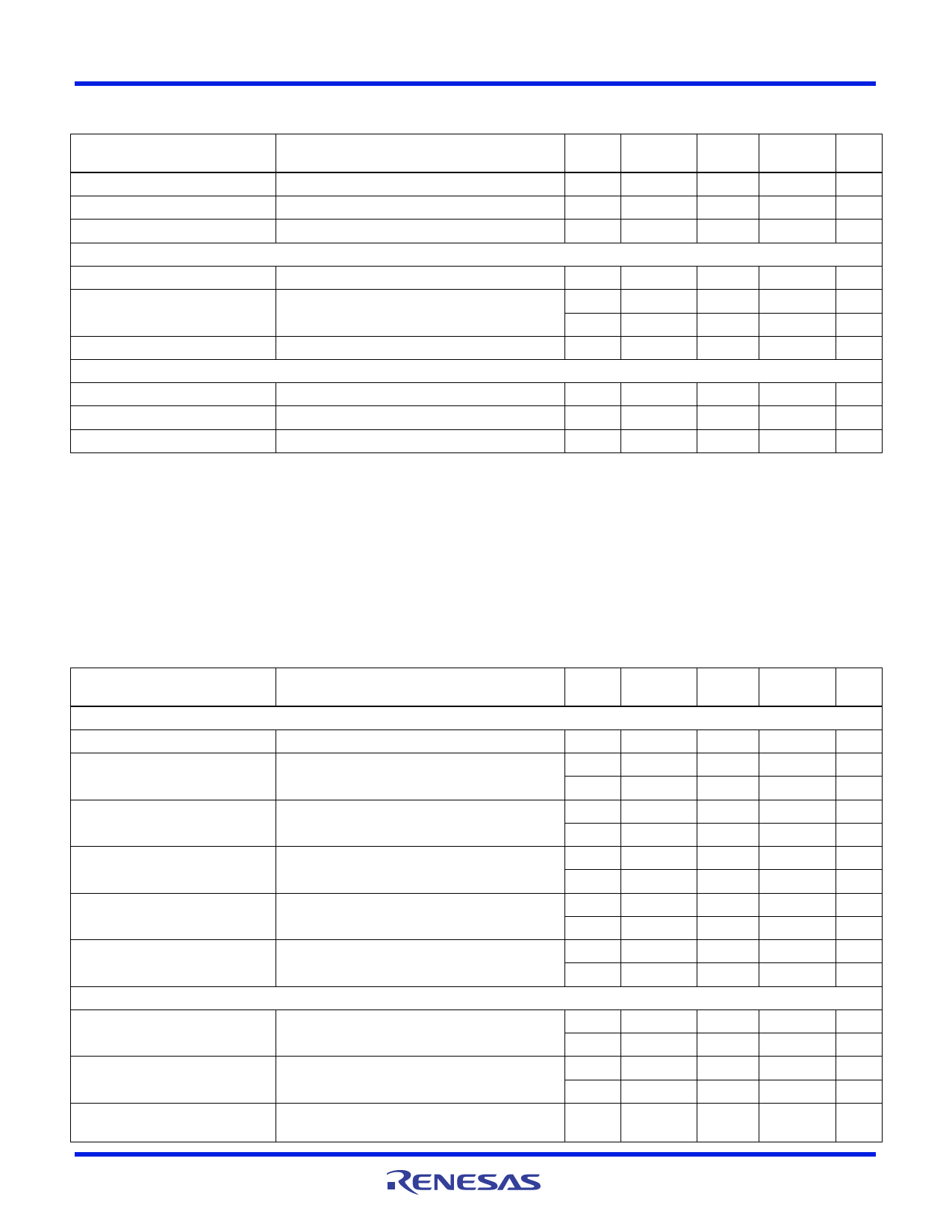
Electrical Specifications - 4.3V Supply
Test Conditions: V+ = +3.9V to +4.5V, GND = 0V, VINH = 1.6V, VINL = 0.5V (Note 6),
Unless Otherwise Specified (Continued)
PARAMETER
TEST CONDITIONS
TEMP
MIN
MAX
(°C) (Notes 7, 8) TYP (Notes 7, 8) UNITS
Total Harmonic Distortion
f = 20Hz to 20kHz, VCOM = 2VPP, RL = 600
25
NO or NC OFF Capacitance, COFF f = 1MHz, VNO or VNC = VCOM = 0V, (See Figure 7) 25
COM ON Capacitance, CCOM(ON) f = 1MHz, VNO or VNC = VCOM = 0V, (See Figure 7) 25
POWER SUPPLY CHARACTERISTICS
-
0.003
-
%
-
106
-
pF
-
212
-
pF
Power Supply Range
Full
1.65
-
4.5
V
Positive Supply Current, I+
V+ = +4.5V, VIN = 0V or V+
25
-
Full
-
-
0.09
A
-
1.4
A
Positive Supply Current, I+
V+ = +4.2V, VIN = 2.85V
DIGITAL INPUT CHARACTERISTICS
25
-
-
12
A
Input Voltage Low, VINL
Full
-
-
0.5
V
Input Voltage High, VINH
Full
1.6
-
-
V
Input Current, IINH, IINL
V+ = 4.5V, VIN = 0V or V+, (Note 10)
Full
-0.5
-
0.5
A
NOTES:
6. VIN = input voltage to perform proper function.
7. The algebraic convention, whereby the most negative value is a minimum and the most positive a maximum, is used in this data sheet.
8. Parts are 100% tested at +25°C. Over-temperature limits established by characterization and are not production tested.
9. Flatness is defined as the difference between maximum and minimum value of ON-Resistance over the specified analog signal range.
10. Limits established by characterization and are not production tested.
11. rON matching between channels is calculated by subtracting the channel with the highest max rON value from the channel with lowest max rON
value, between NC1 and NC2, NC3 and NC4 or between NO1 and NO2, NO3 and NO4.
Electrical Specifications - 3V Supply
Test Conditions: V+ = +2.7V to +3.3V, GND = 0V, VINH = 1.4V, VINL = 0.5V (Note 6),
Unless Otherwise Specified
PARAMETER
TEST CONDITIONS
TEMP
MIN
MAX
(°C) (Notes 7, 8) TYP (Notes 7, 8) UNITS
ANALOG SWITCH CHARACTERISTICS
Analog Signal Range, VANALOG
Full
0
ON-Resistance, rON
V+ = 2.7V, ICOM = 100mA, VNO or VNC = 0V to V+, 25
-
(See Figure 5)
Full
-
-
V+
V
0.3
0.45
-
0.6
rON Matching Between Channels, V+ = 2.7V, ICOM = 100mA, VNO or VNC = Voltage at 25
-
0.04
0.08
rON
max rON, (Note 11)
Full
-
-
0.09
rON Flatness, rFLAT(ON)
V+ = 2.7V, ICOM = 100mA, VNO or VNC = 0V to V+, 25
-
0.06
0.15
(Note 9)
Full
-
-
0.15
NO or NC OFF Leakage Current, V+ = 3.3V, VCOM = 0.3V, 3V, VNO or VNC = 3V, 0.3V 25
-
1.2
-
nA
INO(OFF) or INC(OFF)
Full
-
13
-
nA
COM ON Leakage Current,
V = 3.3V, VCOM = 0.3V, 3V, or VNO or VNC = 0.3V, 25
-
1
-
nA
ICOM(ON)
3V, or Floating
Full
-
35
-
nA
DYNAMIC CHARACTERISTICS
Turn-ON Time, tON
V+ = 2.7V, VNO or VNC = 1.5V, RL = 50,
CL = 35pF, (See Figure 1, Note 10)
25
-
Full
-
21
30
ns
-
35
ns
Turn-OFF Time, tOFF
V+ = 2.7V, VNO or VNC = 1.5V, RL = 50,
CL = 35pF, (See Figure 1, Note 10)
25
-
Full
-
17
27
ns
-
32
ns
Break-Before-Make Time Delay, tD V+ = 3.3V, VNO or VNC = 1.5V, RL = 50,
CL = 35pF, (See Figure 3, Note 10)
Full
2
3
-
ns
FN6111 Rev 3.00
February 5, 2008
Page 4 of 14
Share Link: