74ALVC32PW(2014) データシートの表示(PDF) - NXP Semiconductors.
部品番号
コンポーネント説明
一致するリスト
74ALVC32PW Datasheet PDF : 14 Pages
| |||
Nexperia
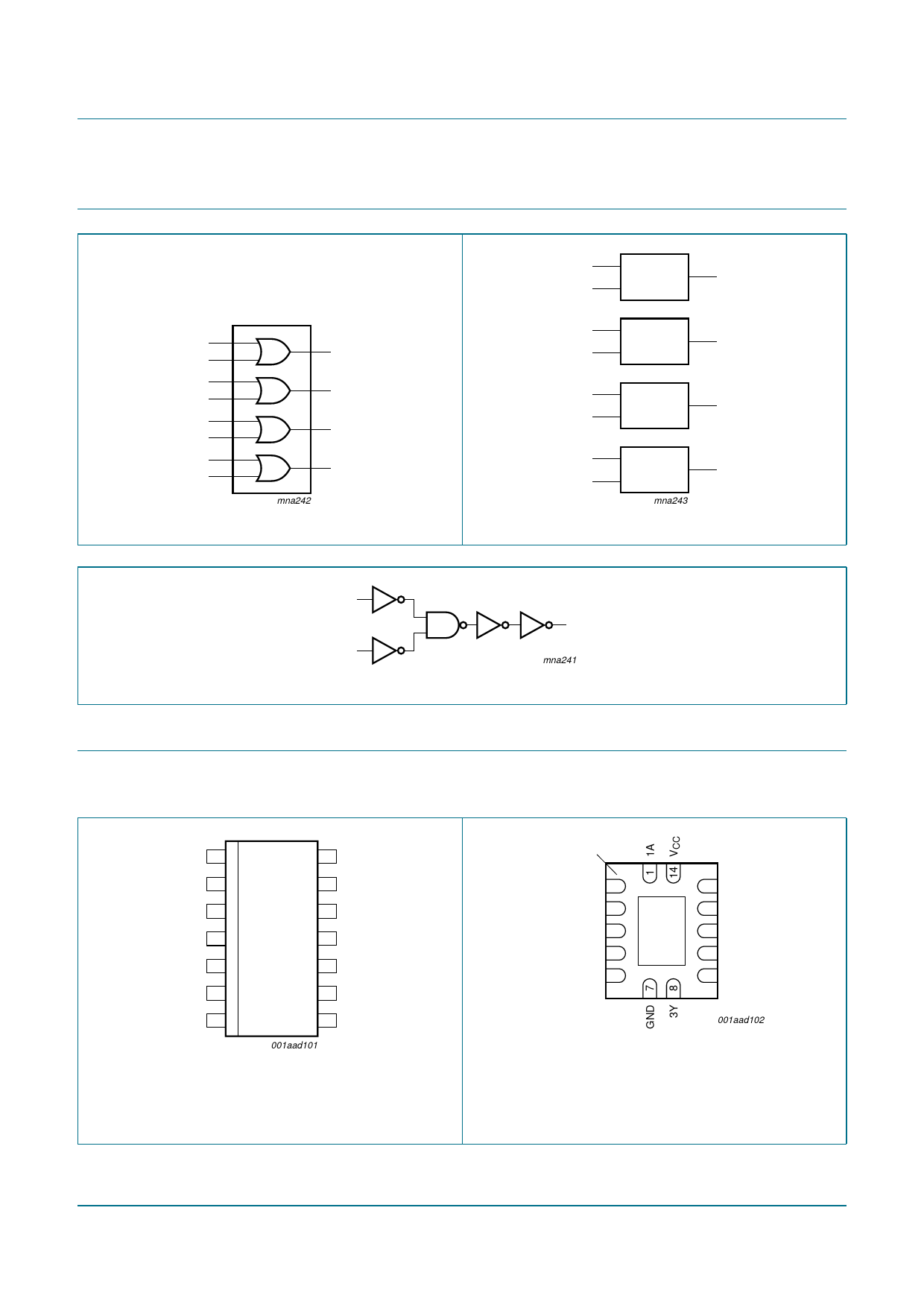
4. Functional diagram
74ALVC32
Quad 2-input OR gate
$
%
$
%
$
%
$
%
Fig 1. Logic symbol
<
<
<
<
PQD
PQD
Fig 2. IEC logic symbol
$
%
Fig 3. Logic diagram (one gate)
5. Pinning information
5.1 Pinning
<
PQD
1A 1
1B 2
1Y 3
2A 4
2B 5
2Y 6
GND 7
14 VCC
13 4B
12 4A
32
11 4Y
10 3B
9 3A
8 3Y
001aad101
Fig 4. Pin configuration SO14 and TSSOP14
terminal 1
index area
1B 2
1Y 3
2A 4
2B 5
2Y 6
32
GND(1)
13 4B
12 4A
11 4Y
10 3B
9 3A
001aad102
Transparent top view
(1) This is not a supply pin. The substrate is attached to this
pad using conductive die attach material. There is no
electrical or mechanical requirement to solder this pad.
However, if it is soldered, the solder land should remain
floating or be connected to GND.
Fig 5. Pin configuration DHVQFN14
74ALVC32
Product data sheet
All information provided in this document is subject to legal disclaimers.
Rev. 3 — 20 January 2014
© Nexperia B.V. 2017. All rights reserved
2 of 14
Share Link: 