MB88151A-500 データシートの表示(PDF) - Unspecified
部品番号
コンポーネント説明
一致するリスト
MB88151A-500 Datasheet PDF : 4 Pages
| |||
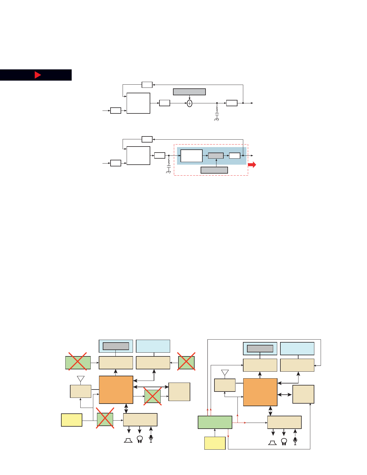
The Fujitsu SSCG
Features
Reference
Clock
I/M
Frequency
Phase
Comparator
1/N
Analog Modulator
CP
Voltage
Accumulator
Analog Method
VCO
Loop Filter
(Capacity)
Outputs the
Clock
I/M
Reference
Clock
Frequency
Phase
CP
Comparator
1/N
V-I
Conversion
IDAC
ICO
Digital Control
Outputs the
Clock
Digital Method
• Digital frequency modulation technique
−Digital control using a current D/A converter
achieves accurate frequency modulation compared
to conventional analog control, which causes
distortion and blunting in the modulated
waveform
• Programmable product (built-in FRAM)
−Set and save output frequency and modulation
parameters by changing the multiplication /
division clock rate
• Single input and multiple outputs (Max. 8 Clock
outputs, Example: MB88181)
−One device supports multiple clocks, thus reducing
the need for other components such as oscillators
• Selectable modulation rate
−No modulation, ±0.5%, ±1.0%, ±2.0%, -1.0%,
-2.0%, -4.0%
• Enhanced input frequency range
−8.3MHz to 134MHz
• Low current consumption
−5.5mA @ 25MHz
• Power supply voltage range
−1.65 V to 3.6 V
• Pin compatibility with other products in the market
• Package options
−SOP8, TSSOP8, BCC6, BCC18, BCC20
XTAL
27.12MHz
RF
3V
Conventional
LCD
LCDC
3V
Video/image
Control
DSP
3V
XTAL
37MHz
System
LSI
3V
48MHz Level
Shifter
USB
1.8V
The Fujitsu SSCG Solution
Reduces BOM cost and PCB area
CLK O/P1 37MHz
LCD
Video/image
Control
CLK O/P2 27.12MHz
LCDC
3V
DSP
3V
RF
3V
System
LSI
3V
USB
1.8V
TCXO
19.2MHz
Buffer
Audio
3V
SSCG
CLK O/P3 19.2MHz
TCXO
19.2MHz
CLK O/P4 48MHz
Audio
3V
Share Link: 