SL74HC299 データシートの表示(PDF) - System Logic Semiconductor
部品番号
コンポーネント説明
一致するリスト
SL74HC299
System Logic Semiconductor

SL74HC299 Datasheet PDF : 8 Pages
| |||
SL74HC299
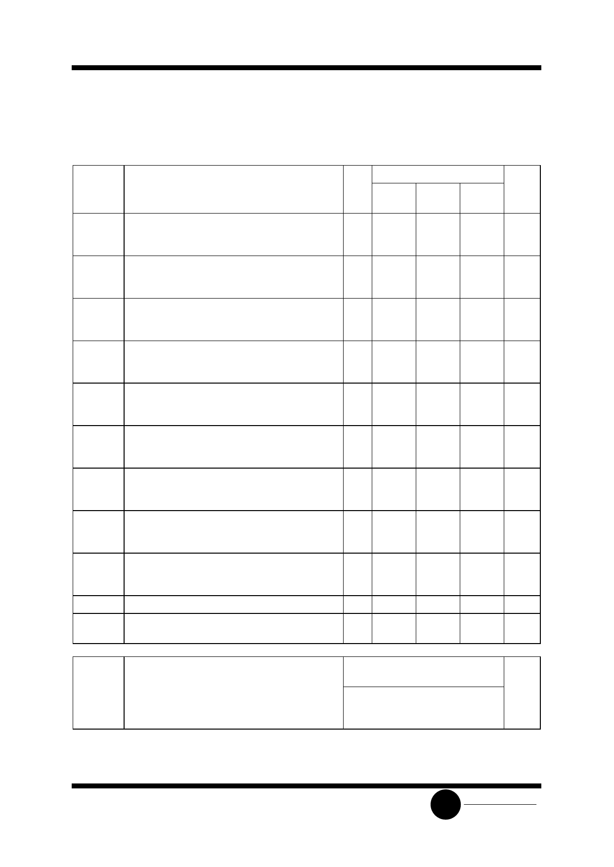
AC ELECTRICAL CHARACTERISTICS(CL=50pF,Input tr=tf=6.0 ns)
Symbol
Parameter
fmax Maximum Clock Frequency (50% Duty Cycle)
(Figures 1 and 5)
tPLH, tPHL Maximum Propagation Delay, Clock to QA’ or QH’
(Figures 1 and 5)
tPLH, tPHL Maximum Propagation Delay, Clock to QA thru QH
(Figures 1 and 5)
tPHL Maximum Propagation Delay, Reset to QA’ or QH’
(Figures 2 and 5)
tPHL Maximum Propagation Delay, Reset to QA thru QH
(Figures 2 and 5)
tPLZ, tPHZ Maximum Propagation Delay , OE1, OE2, S1, or S2
to QA thru QH (Figures 3 and 6)
tPZL, tPZH Maximum Propagation Delay , OE1, OE2, S1, or S2
to QA thru QH (Figures 3 and 6)
tTLH, tTHL Maximum Output Transition Time, QA thru QH
(Figures 1 and 5)
tTLH, tTHL Maximum Output Transition Time, QA’ thru QH’
(Figures 1 and 5)
CIN
Maximum Input Capacitance)
COUT Maximum Three-State I/O Capacitance
(I/O in High-Impedance State), QA thru QH
VCC
Guaranteed Limit
V 25 °C to ≤85°C ≤125°C
-55°C
2.0 5.0
4.0
3.4
4.5 25
20
17
6.0 29
24
20
2.0 170
215
255
4.5 34
43
51
6.0 29
37
43
2.0 160
200
240
4.5 32
40
48
6.0 27
34
41
2.0 175
220
265
4.5 35
44
53
6.0 30
37
45
2.0 190
240
285
4.5 38
48
57
6.0 32
41
48
2.0 150
190
225
4.5 30
38
45
6.0 26
33
38
2.0 150
190
225
4.5 30
38
45
6.0 26
33
38
2.0 60
75
90
4.5 12
15
18
6.0 10
13
15
2.0 75
95
110
4.5 15
19
22
6.0 13
16
19
-
10
10
10
-
15
15
15
Unit
MHz
ns
ns
ns
ns
ns
ns
ns
ns
pF
pF
Power Dissipation Capacitance (Per Package),
Output Enable
CPD Used to determine the no-load dynamic power
consumption:
PD=CPDVCC2f+ICCVCC
Typical @25°C,VCC=5.0 V
240
pF
SLS
System Logic
Semiconductor
Share Link: