MB88154A データシートの表示(PDF) - Cypress Semiconductor
部品番号
コンポーネント説明
一致するリスト
MB88154A Datasheet PDF : 24 Pages
| |||
MB88154A
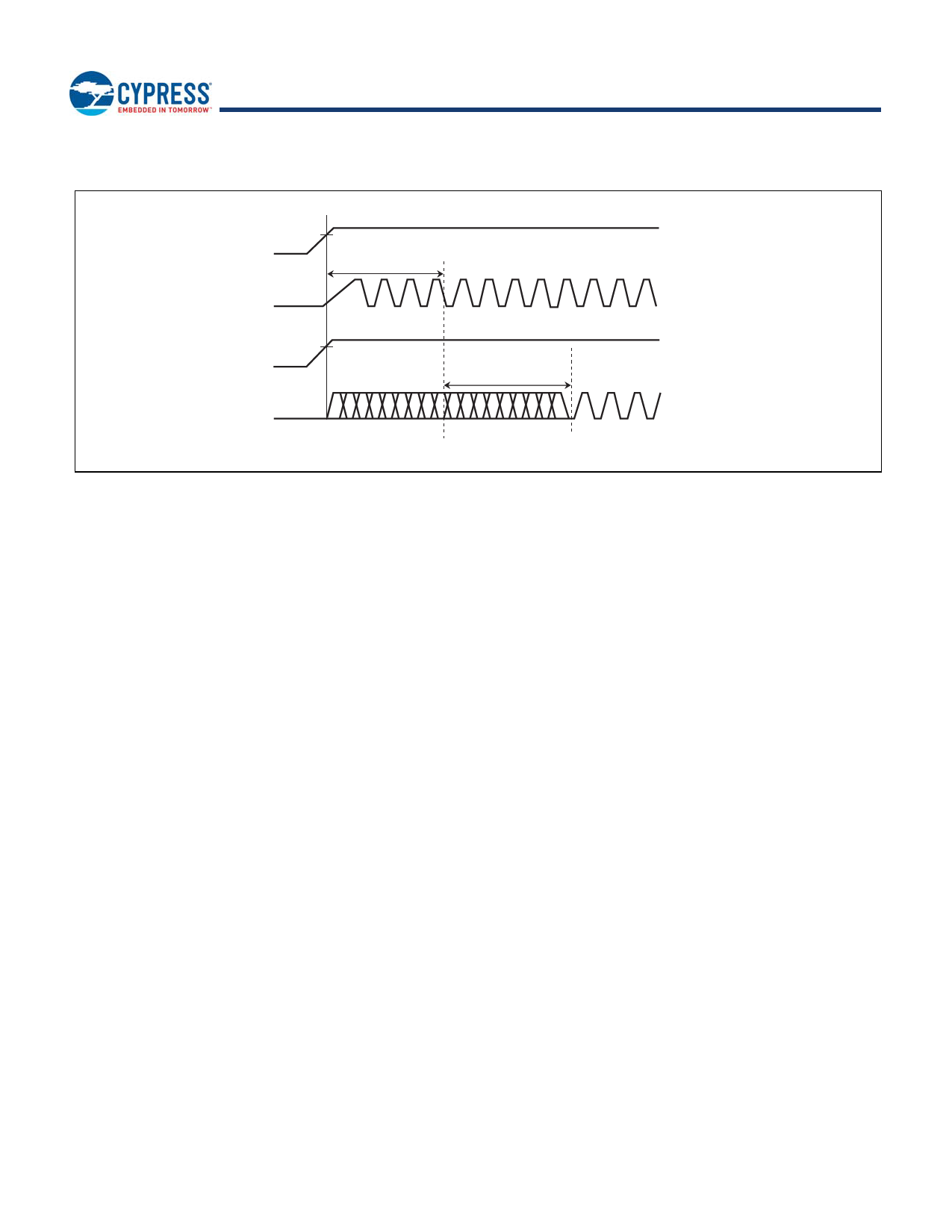
16. Lock-up Time
VDD
3.0 V
Internal clock
stabilization wait time
XIN
Setting pin VIH
SEL0,
SEL1
CKOUT
tLK
(lock-up time )
If the setting pin is fixed at the “H” or “L” level, the maximum time after the power is turned on until the set clock signal is output from
CKOUT pin is (the stabilization wait time of input clock to XIN pin) + (the lock-up time “tLK”). For the input clock stabilization time,
check the characteristics of the resonator or oscillator used.
Note : When the pin setting is changed, the CKOUT pin output clock stabilization time is required. Until the output clock signal
becomes stable, the output frequency, output clock duty cycle, modulation period, and cycle-cycle jitter cannot be guaranteed.
It is therefore advisable to perform processing such as cancelling a reset of the device at the succeeding stage after
the lock-up time.
Document Number: 002-08252 Rev. *B
Page 16 of 23
Share Link: 