NJU3102G データシートの表示(PDF) - Japan Radio Corporation
部品番号
コンポーネント説明
一致するリスト
NJU3102G Datasheet PDF : 22 Pages
| |||
NJU3102
• PORTD(PD0−PD3)
PORTD is a 4-bit input-output PORT. When the PORT is set as the output, the signal is output through
the output terminal by writing data to the PORTD register(PHY4). When the PORT is set as the input,
the external signal is gotten directly through the input terminal by reading data from PHY4.
Though the output circuit is Nch open drain type, the C-MOS input buffer is connected to the same
terminal. Therefore, the operating current of the chip by the short circuit current when the middle level
voltage between VDD and VSS is input to this terminal.
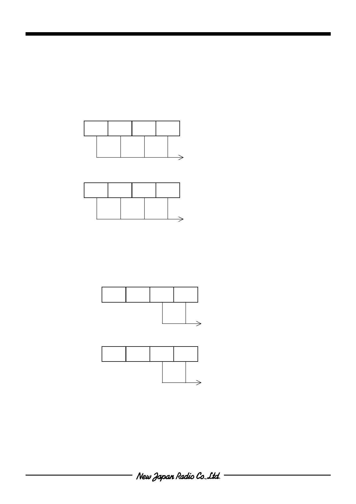
[READING PORTD INPUT DATA (PHY4)]
(MSB) 3
2
1
0
(LSB)
PHY4 PD3 PD2 PD1 PD0
PORTD Input Data
[WRITING PORTD OUTPUT DATA (PHY4)]
(MSB) 3
2
1
0 (LSB)
PHY4 PD3 PD2 PD1 PD0
PORTD Output Data
• PORTE(PE0, PE1)
PORTE is a 2-bit input-output PORT. When the PORT is set as the output, the signal is output through
the output terminal by writing data to the PORTE register(PHY5). When the PORT is set as the input,
the external signal is gotten directly through the input terminal by reading data from PHY5.
[READING PORTE INPUT DATA (PHY5)]
(MSB) 3
2
1
PHY5
“0”
“0”
PE1
0 (LSB)
PE0
[WRITING PORTE OUTPUT DATA (PHY5)]
(MSB) 3
2
1
PHY5
–
–
PE1
PORTE Input Data
0 (LSB)
PE0
PORTE Output Data
- 10 -
Share Link: 