M74HC692 データシートの表示(PDF) - STMicroelectronics
部品番号
コンポーネント説明
一致するリスト
M74HC692 Datasheet PDF : 17 Pages
| |||
M74HC692
DECADE COUNTER/REGISTER (3-STATE)
s HIGH SPEED:
fMAX = 53 MHz (TYP.) at VCC = 6V
s LOW POWER DISSIPATION:
ICC = 4µA(MAX.) at TA=25°C
s HIGH NOISE IMMUNITY:
VNIH = VNIL = 28 % VCC (MIN.)
s SYMMETRICAL OUTPUT IMPEDANCE:
|IOH| = IOL = 6mA (MIN) for QA to QD OUTPUT
|IOH| = IOL = 4mA (MIN) for RCO OUTPUT
s BALANCED PROPAGATION DELAYS:
tPLH ≅ tPHL
s WIDE OPERATING VOLTAGE RANGE:
VCC (OPR) = 2V to 6V
s PIN AND FUNCTION COMPATIBLE WITH
74 SERIES 692
DESCRIPTION
The M74HC692 is an high speed CMOS
DECADE/COUNTER REGISTER (3 STATE)
fabricated with silicon gate C2MOS technology.
The internal circuit is composed of 3 stages
including buffer output, which offers high noise
immunity and stable output. This device
incorporates a synchronous counter, four bit
D-type register, and quadruple two-line to one-line
multiplexers with three-state outputs in a single 20
pin package. The counter can be programmed
from the data inputs and have enable P and
enable T inputs and a ripple carry output for easy
expansion. The register/counter select input, R/C,
selects the counter when low or the register when
high for the three state-outputs, QA, QB, QC, and
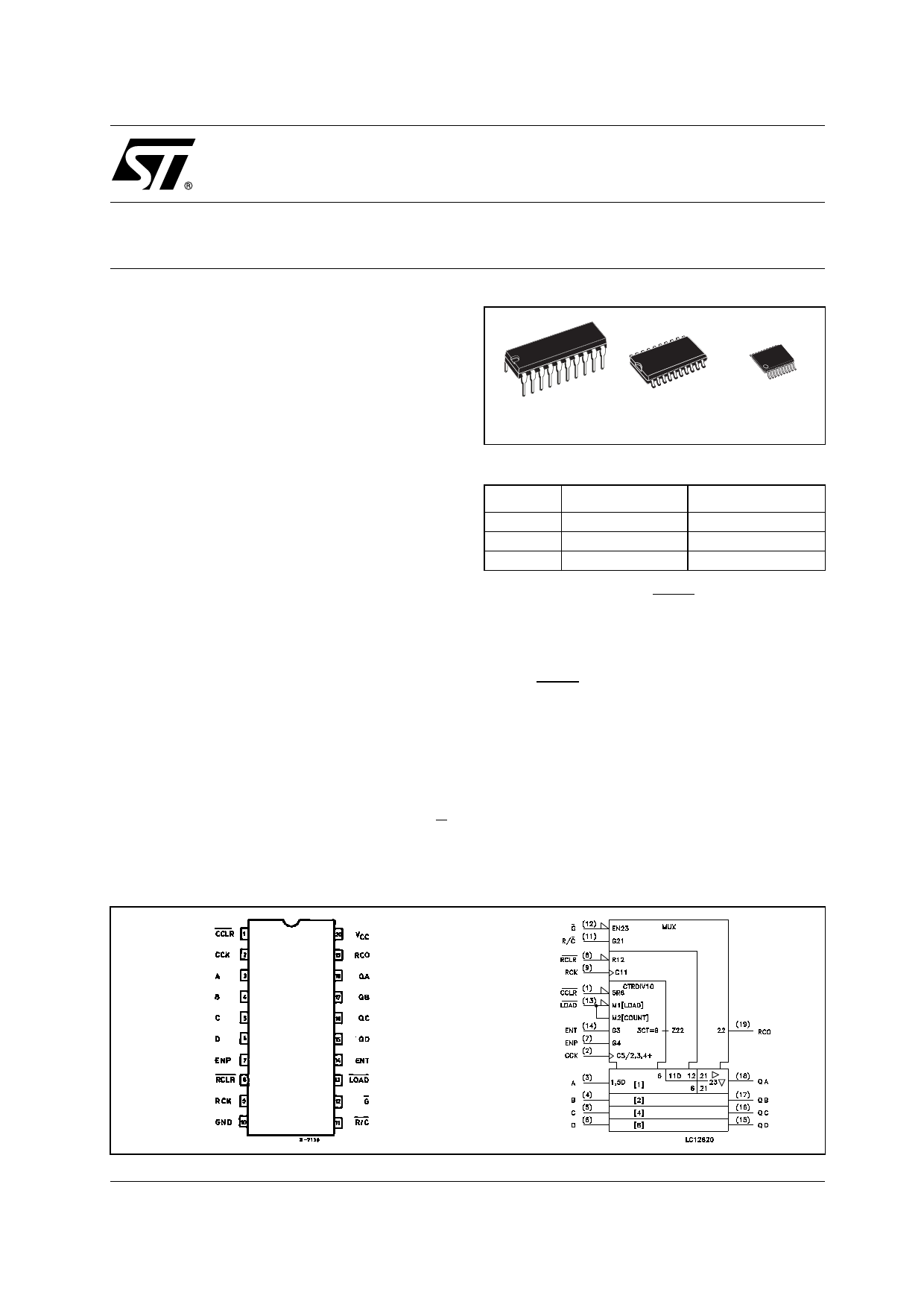
PIN CONNECTION AND IEC LOGIC SYMBOLS
DIP
SOP
TSSOP
ORDER CODES
PACKAGE
TUBE
DIP
SOP
TSSOP
M74HC692B1R
M74HC692M1R
T&R
M74HC692RM13TR
M74HC692TTR
QD. If the LOAD input (LOAD) is held "L" DATA
input (A - D) are loaded into the internal counter at
positive edge of counter clock input (CCK). In the
counter mode, internal counter counts up at the
positive of the counter clock. If the counter clear
inputs (CCLR) is held "L", the internal counter is
cleared synchronously to the counter clock. The
internal counter’s outputs are stored in the output
register at the positive edge of the register clock
(RCK). If the register clear input (RCLR) is held "L"
the register is cleared synchronously to register
clock.
All inputs are equipped with protection circuits
against static discharge and transient excess
voltage.
August 2001
1/17
Share Link: 