EL7564 データシートの表示(PDF) - Renesas Electronics
部品番号
コンポーネント説明
一致するリスト
EL7564 Datasheet PDF : 17 Pages
| |||
EL7564
Pin Descriptions
20-PIN SO
(0.300”)
28-PIN
HTSSOP
1
1
2
2
3
3
4
4
5
5
6, 7
6, 7, 8, 9
8
10, 11
9
13
10
14
11, 12, 13
15, 16
14, 15
16
18, 19, 20, 21,
22, 23
24
17
25
18
26
19
27
20
28
PIN NAME
VREF
SGND
COSC
VDD
VTJ
PGND
VIN
STP
STN
PGND
LX
VHI
VDRV
PG
FB
EN
PIN FUNCTION
Bandgap reference bypass capacitor; typically 0.1µF to SGND
Control circuit negative supply or signal ground
Oscillator timing capacitor (see performance curves)
Control circuit positive supply; normally connected to VIN through an RC filter
Junction temperature monitor; connected with 2.2nF to 3.3nF to SGND
Ground return of the regulator; connected to the source of the low-side synchronous NMOS
power FET
Power supply input of the regulator; connected to the drain of the high-side NMOS power FET
Auxiliary supply tracking positive input; tied to regulator output to synchronize start up with a
second supply; leave open for stand alone operation; 2µA internal pull down current
Auxiliary supply tracking negative input; connect to output of a second supply to synchronize
start up; leave open for stand alone operation; 2µA internal pull up current
Ground return of the regulator; connected to the source of the low-side synchronous NMOS
power FET
Inductor drive pin; high current output whose average voltage equals the regulator output
voltage
Positive supply of high-side driver; boot strapped from VDRV to LX with an external 0.22µF
capacitor
Positive supply of low-side driver and input voltage for high side boot strap
Power good window comparator output; logic 1 when regulator output is within ±10% of target
output voltage
Voltage feedback input; connected to external resistor divider between VOUT and SGND; a
125nA pull-up current forces VOUT to SGND in the event that FB is floating
Chip enable, active high; a 2µA internal pull up current enables the device if the pin is left open;
a capacitor can be added at this pin to delay the start of converter
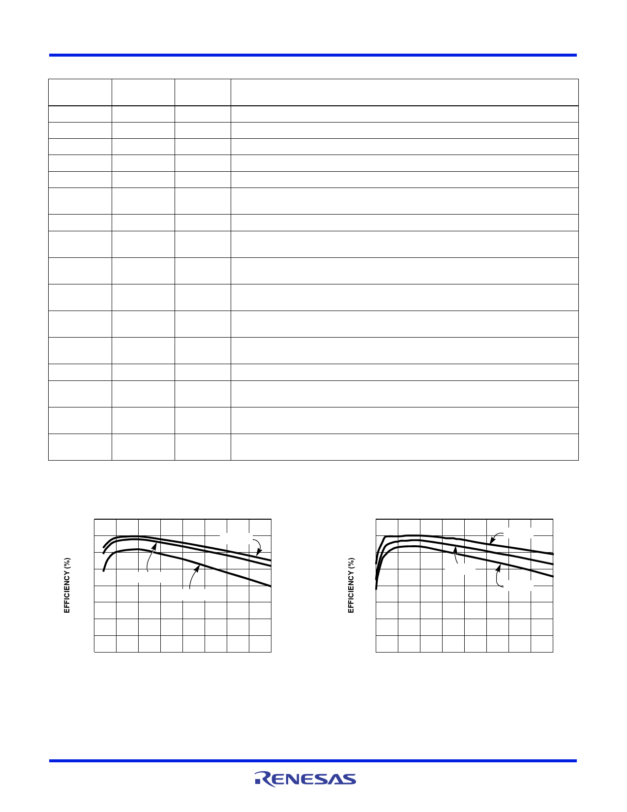
Typical Performance Curves
VIN=5V
100
95
VO=3.3V
90
85
VO=2.8V
80
VO=1.8V
75
70
65
600
0.5
1
1.5
2
2.5
3
3.5
4
LOAD CURRENT IO (A)
FIGURE 1. EL7564CM EFFICIENCY
VIN=5V
100
95
VO=3.3V
90
85
VO=2.5V
80
VO=1.8V
75
70
65
60
0.1 0.6 1.1 1.6 2.1 2.6 3.1 3.6 4.1
IO (A)
FIGURE 2. EL7564CRE EFFICIENCY
FN7297 Rev 3.00
May 9, 2005
Page 5 of 17
Share Link: 