HIP1011BCB データシートの表示(PDF) - Renesas Electronics
部品番号
コンポーネント説明
一致するリスト
HIP1011BCB Datasheet PDF : 9 Pages
| |||
HIP1011B
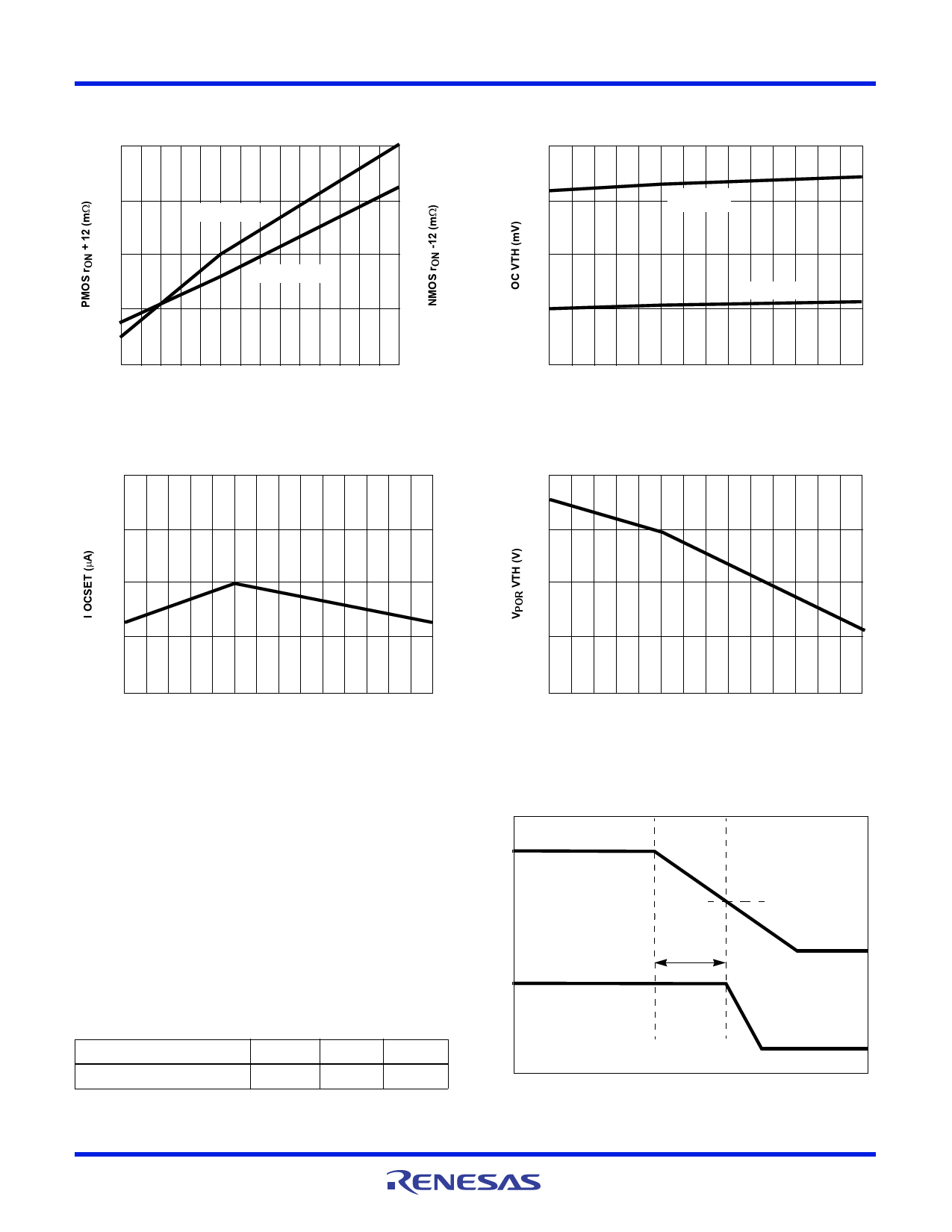
Typical Performance Curves
340
1000
320
900
NMOS -12 rON
300
800
PMOS +12 rON
280
700
260
0
600
5 10 15 20 25 30 35 40 45 50 55 60 65 70
TEMPERATURE (oC)
FIGURE 1. rON vs TEMPERATURE
102
101
100
99
98
0 5 10 15 20 25 30 35 40 45 50 55 60 65 70
TEMPERATURE (oC)
FIGURE 3. OCSET CURRENT vs TEMPERATURE
Adjusting the Fault Reporting and Power
Supply Latch-Off Delay Times
Figure 5 illustrates the relationship between the FLTN signal
and the gate drive outputs. Duration a, indicates the time
between FLTN starting to transition from High to Low,
(indicating a fault has occurred) and the start of the gate
drive outputs latching off. The latch-off is initiated by the
falling FLTN signal reaching the output latch threshold
voltage, VFLTN, TH. For additional details and wave forms
see HIP1011A Data Sheet FN4631. Table 1 illustrates the
effect of the FLTN capacitor on the response times.
TABLE 1. RESPONSE TIME TABLE
3V5VG Response a
0.001F
0.85s
0.1F
37s
10F
3.8ms
FN4640 Rev 5.00
November 18, 2004
105
95
3V OCVTH
85
5V OCVTH
75
65
0 5 10 15 20 25 30 35 40 45 50 55 60 65 70
TEMPERATURE (oC)
FIGURE 2. OC VTH vs TEMPERATURE (VROCSET = 1.21V)
9.5
9.4
9.3
9.2
9.1
0
5 10 15 20 25 30 35 40 45 50 55 60 65 70
TEMPERATURE (oC)
FIGURE 4. VCC POWER ON RESET VTH vs TEMPERATURE
VFLTN,TH
FLTN
a
3V5VG
T1
T2
FIGURE 5. TIMING DIAGRAM
Page 6 of 9
Share Link: 