V827332N04SXTL-A1 データシートの表示(PDF) - Mosel Vitelic Corporation
部品番号
コンポーネント説明
一致するリスト
V827332N04SXTL-A1
Mosel Vitelic Corporation

V827332N04SXTL-A1 Datasheet PDF : 15 Pages
| |||
MOSEL VITELIC
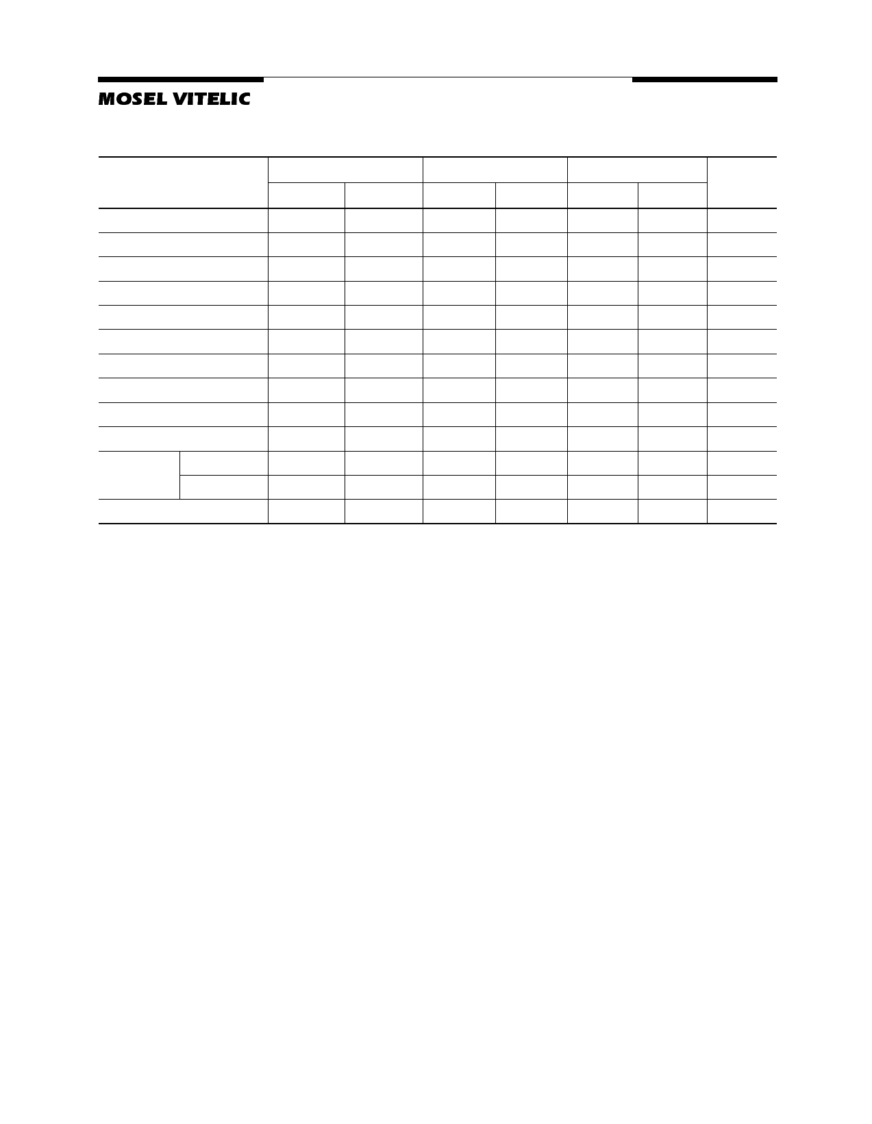
V827332N04S
DDR SDRAM IDD SPEC TABLE
Symbol
A1(PC1600@CL=2)
Typical
Worst
IDD0
1450
1440
IDD1
1650
1710
IDD2P
750
720
IDD2F
895
945
IDD2Q
830
810
IDD3P
980
765
IDD3N
900
990
IDD4R
1980
2250
IDD4W
2115
2385
IDD5
2115
2385
IDD6
Normal
36
36
Low power
18
18
IDD7
3375
3825
B0(PC2100B@CL=2.5) B1(PC2100A@CL=2)
Typical
Worst Typical Worst
1350
1440
1080
1170
1575
1710
1280
1395
675
720
540
585
655
945
720
765
765
810
630
675
720
765
585
630
900
990
720
810
1980
2250
1620
1845
2115
2385
1710
1890
2115
2385
1710
1890
36
36
36
36
18
18
18
18
3375
3825
2745
3150
Unit
mA
mA
mA
mA
mA
mA
mA
mA
mA
mA
mA
mA
mA
* Module IDD was calculated on the basis of component IDD and can be differently measured according to DQ loading cap.
Detailed test conditions for DDR SDRAM IDD1 & IDD
IDD1 : Operating current: One bank operation
1. Typical Case : Vdd = 2.5V, T=25’ C
2. Worst Case : Vdd = 2.7V, T= 10’ C
3. Only one bank is accessed with tRC(min), Burst Mode, Address and Control inputs on NOP edge are changing once
per clock cycle. lout = 0mA
4. Timing patterns
- DDR200(100Mhz, CL=2) : tCK = 10ns, CL2, BL=4, tRCD = 2*tCK, tRAS = 5*tCK
Read : A0 N R0 N N P0 N A0 N - repeat the same timing with random address changing
*50% of data changing at every burst
- DDR266B(133Mhz, CL=2.5) : tCK = 7.5ns, CL=2.5, BL=4, tRCD = 3*tCK, tRC = 9*tCK, tRAS = 5*tCK
Read : A0 N N R0 N P0 N N N A0 N - repeat the same timing with random address changing
*50% of data changing at every burst
- DDR266A (133Mhz, CL=2) : tCK = 7.5ns, CL=2, BL=4, tRCD = 3*tCK, tRC = 9*tCK, tRAS = 5*tCK
Read : A0 N N R0 N P0 N N N A0 N - repeat the same timing with random address changing
*50% of data changing at every burst
Legend : A=Activate, R=Read, W=Write, P=Precharge, N=NOP
V827332N04S Rev. 1.1 May 2002
9
Share Link: