EL7516IY データシートの表示(PDF) - Renesas Electronics
部品番号
コンポーネント説明
一致するリスト
EL7516IY Datasheet PDF : 12 Pages
| |||
EL7516
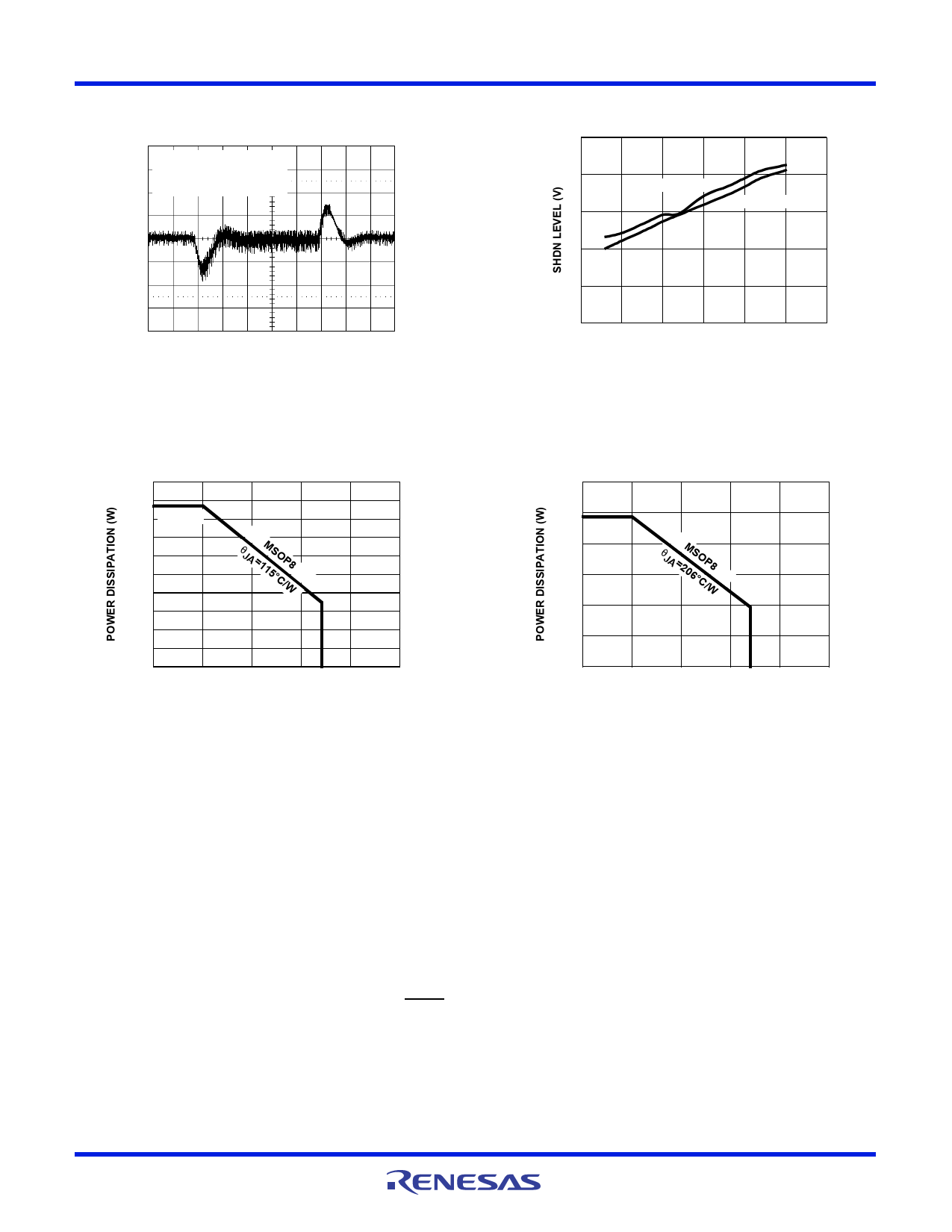
Typical Performance Curves (Continued)
VIN = 3.3V
VOUT = 12V
IOUT = 50mA TO 300mA
200mV/DIV
0.1ms/DIV
FIGURE 25. TRANSIENT RESPONSE - 1.2MHz
5
4
SHDN TURN ON
SHDN TURN OFF
3
2
1
0
3
3.5
4
4.5
5
5.5
6
VIN (V)
FIGURE 26. TYPICAL SHDN INPUT LEVEL vs VIN
JEDEC JESD51-7 HIGH EFFECTIVE THERMAL
CONDUCTIVITY TEST BOARD
1.0
0.9
0.8 870mW
0.7
0.6
0.5
0.4
JA =11M5S°OC/PW8
0.3
0.2
0.1
0
0
25
50
75 85 100
125
AMBIENT TEMPERATURE (°C)
FIGURE 27. PACKAGE POWER DISSIPATION vs AMBIENT
TEMPERATURE
Applications Information
The EL7516 is a high frequency, high efficiency boost
regulator operated at constant frequency PWM mode. The
boost converter stores energy from an input voltage source
and delivers it to a higher output voltage. The input voltage
range is 2.5V to 5.5V and the output voltage range is 5V to
18V. The switching frequency is selectable between 600KHz
and 1.2MHz, allowing smaller inductors and faster transient
response. An external compensation pin gives the user
greater flexibility in setting output transient response and
tighter load regulation. The converter soft-start characteristic
can also be controlled by external CSS capacitor. The SHDN
pin allows the user to completely shut-down the device.
Boost Converter Operations
Figure 28 shows a boost converter with all the key
components. In steady state operating and continuous
conduction mode where the inductor current is continuous,
FN7333 Rev 6.00
October 9, 2007
JEDEC JESD51-3 LOW EFFECTIVE THERMAL
CONDUCTIVITY TEST BOARD
0.6
0.5
486mW
0.4
0.3
0.2
JA =2M06S°OCP/W8
0.1
0
0
25
50
75 85 100
125
AMBIENT TEMPERATURE (°C)
FIGURE 28. PACKAGE POWER DISSIPATION vs AMBIENT
TEMPERATURE
the boost converter operates in two cycles. During the first
cycle, as shown in Figure 29, the internal power FET turns
on and the Schottky diode is reverse biased and cuts off the
current flow to the output. The output current is supplied
from the output capacitor. The voltage across the inductor is
VIN and the inductor current ramps up in a rate of VIN / L, L
is the inductance. The inductance is magnetized and energy
is stored in the inductor. The change in inductor current is:
IL1 = t1 -V---L-I--N--
t1 = -f-S--D--W----
D = Duty Cycle
VO = C--I--O-O---U--U--T--T- t1
(EQ. 1)
Page 8 of 12
Share Link: 