P4C187-25LMB データシートの表示(PDF) - Semiconductor Corporation
部品番号
コンポーネント説明
一致するリスト
P4C187-25LMB Datasheet PDF : 12 Pages
| |||
P4C187/187L
AC CHARACTERISTICS—READ CYCLE
(VCC = 5V ± 10%, All Temperature Ranges)(2)
Symbol Parameter
tRC Read Cycle Time
tAA Address Access Time
tAC Chip Enable Access Time
tOH Output Hold from Address Change
tLZ Chip Enable to Output in Low Z
tHZ Chip Disable to Output in High Z
tPU Chip Enable to Power Up Time
tPD Chip Disable to Power Down Time
-10
-12
-15
-20
-25
-35
-45
-55
-70
-85
Min Max Min Max Min Max Min Max Min Max Min Max Min Max Min Max Min Max Min Max
10
12
15
20
25
35
45
55
70
85
10
12
15
20
25
35
45
55
70
85
10
12
15
20
25
35
45
65
70
85
2
2
2
2
2
2
2
2
2
2
2
2
2
2
2
2
2
2
2
2
5
6
8
10
12
17
20
25
30
35
0
0
0
0
0
0
0
0
0
0
10
12
15
20
25
35
45
55
70
85
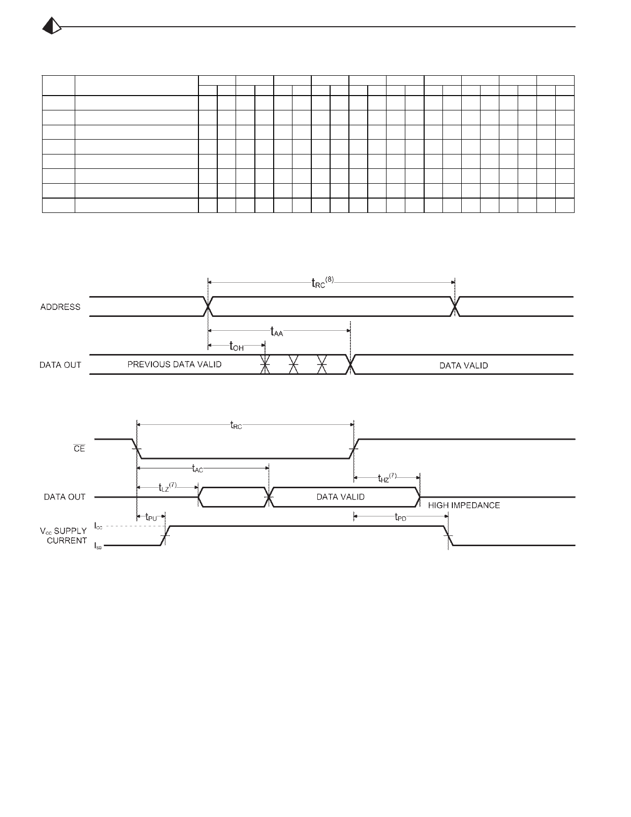
TIMING WAVEFORM OF READ CYCLE NO. 1(5)
TIMING WAVEFORM OF READ CYCLE NO. 2(6)
Notes:
5. CE is LOW and WE is HIGH for READ cycle.
6. WE is HIGH, and address must be valid prior to or coincident with CE
transition LOW.
7. Transition is measured ±200mV from steady state voltage prior to
change with specified loading in Figure 1. This parameter is sampled
and not 100% tested.
8. Read Cycle Time is measured from the last valid address to the first
transitioning address.
Document # SRAM111 REV B
Page 4 of 12
Share Link: 