ISL8011 データシートの表示(PDF) - Renesas Electronics
部品番号
コンポーネント説明
一致するリスト
ISL8011 Datasheet PDF : 10 Pages
| |||
ISL8011
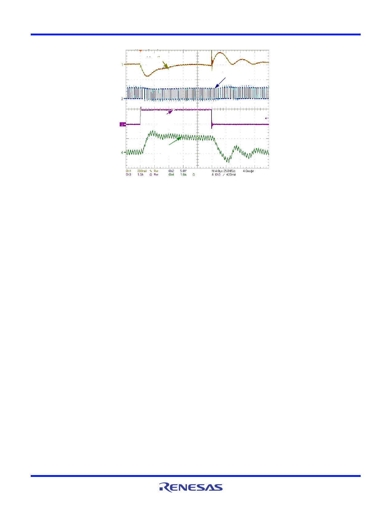
Typical Operating Performance (Continued)
VOUT
VPHASE
IO
IL
FIGURE 9. LOAD TRANSIENT (VIN = 3.6V; VO = 1.6V; IO = 0A TO ~1A)
Pin Descriptions
PVIN
Input supply voltage. Connect a 10µF ceramic capacitor to
power ground.
VCC
Supply voltage for internal analog and digital control circuits,
delivered from PVIN. Bypass with 0.1µF ceramic capacitor to
signal ground.
EN
Regulator enable pin. Force this pin above 1.4V enable the
chip. Force this pin below 0.4V shutdown the chip and
discharge output capacitor when driven to low. Do not leave
this pin floating.
POR
200ms timer output. At power-up or EN HI, this output is a
200ms delayed Power-Good signal for the output voltage.
GND
Ground. Connect this pin to the exposed pad and SGND.
PHASE
Switching node connection. Connect to one terminal of
inductor.
PGND
Power ground. Connect all power grounds to this pin.
SGND
Analog ground. SGND and PGND should only have one
point connection.
FB
Buck regulator output feedback. Connect to the output
through a resistor divider for adjustable the output voltage.
Exposed Pad
The exposed pad must be connected to the PGND pin for
proper electrical performance and optimal thermal
performance.
NC
NC is the No Connect pin. Tie this pin to SGND to prevent
noise.
FN9254 Rev 2.00
August 4, 2009
Page 5 of 10
Share Link: 