ISL84524 データシートの表示(PDF) - Renesas Electronics
部品番号
コンポーネント説明
一致するリスト
ISL84524 Datasheet PDF : 13 Pages
| |||
ISL84524, ISL84525
Leakage Considerations
Reverse ESD protection diodes are internally connected
between each analog-signal pin and both V+ and GND. One of
these diodes conducts if any analog signal exceeds V+ or
GND.
Virtually all the analog leakage current comes from the ESD
diodes to V+ or GND. Although the ESD diodes on a given
signal pin are identical and therefore fairly well balanced,
they are reverse biased differently. Each is biased by either
V+ or GND and the analog signal. This means their leakages
will vary as the signal varies. The difference in the two diode
leakages to the V+ and GND pins constitutes the
analog-signal-path leakage current. All analog leakage
current flows between each pin and one of the supply
terminals, not to the other switch terminal. This is why both
sides of a given switch can show leakage currents of the
same or opposite polarity. There is no connection between
the analog signal paths and V+ or GND.
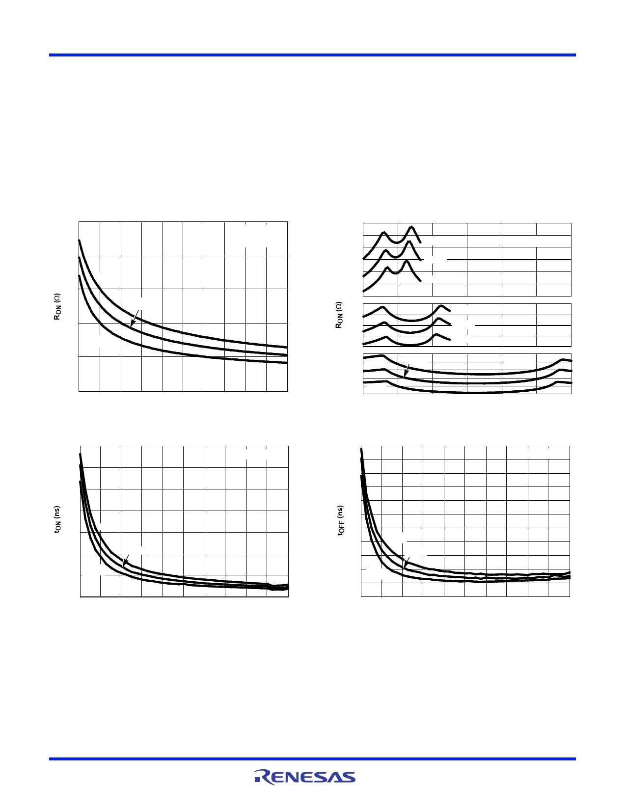
Typical Performance Curves TA = +25°C, Unless Otherwise Specified
250
200
+85°C
150
+25°C
100
-40°C
50
VCOM = (V+) - 1V
ICOM = 1mA
0
3 4 5 6 7 8 9 10 11 12 13
V+ (V)
FIGURE 9. ON RESISTANCE vs SUPPLY VOLTAGE
225
200
175
+85°C
V+ = 3.3V
ICOM = 1mA
150
+25°C
125
100
-40°C
75
140
120
+85°C
V+ = 5V
100
+25°C
80
-40°C
60
80
70 +85°C
+25°C
V+ = 12V
60
50
40 -40°C
30
0
2
4
6
8
10
12
VCOM (V)
FIGURE 10. ON RESISTANCE vs SWITCH VOLTAGE
350
VCOM = (V+) - 1V
300
250
200
150
+85°C
100
50 -40°C
+25°C
0
2 3 4 5 6 7 8 9 10 11 12
V+ (V)
FIGURE 11. TURN - ON TIME vs SUPPLY VOLTAGE
120
110
VCOM = (V+) - 1V
100
90
80
70
60
50
+85°C
40
+25°C
30
-40°C
20
10
2 3 4 5 6 7 8 9 10 11 12
V+ (V)
FIGURE 12. TURN - OFF TIME vs SUPPLY VOLTAGE
FN6042 Rev 3.00
February 24, 2012
Page 10 of 13
Share Link: 