MM74C32 データシートの表示(PDF) - Fairchild Semiconductor
部品番号
コンポーネント説明
一致するリスト
MM74C32 Datasheet PDF : 4 Pages
| |||
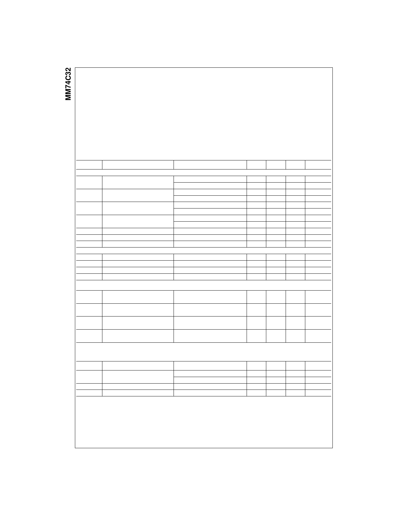
Absolute Maximum Ratings(Note 1)
Voltage at Any Pin
Operating Temperature Range
Storage Temperature Range
Power Dissipation (PD)
Dual-In-Line
Small Outline
Operating VCC Range
−0.3V to VCC + 0.3V
−40°C to +85°C
−65°C to +150°C
700 mW
500 mW
3.0V to 15V
Absolute Maximum VCC
18V
Lead Temperature
(Soldering, 10 seconds)
260°C
Note 1: “Absolute Maximum Ratings” are those values beyond which the
safety of the device cannot be guaranteed. Except for “Operating Tempera-
ture Range” they are not meant to imply that the devices should be oper-
ated at these limits. The Electrical Characteristics table provides conditions
for actual device operation.
DC Electrical Characteristics
Min/Max limits apply across temperature range unless otherwise noted
Symbol
Parameter
Conditions
Min
Typ
Max
CMOS TO CMOS
VIN(1)
Logical “1” Input Voltage
VIN(0)
Logical “0” Input Voltage
VOUT(1)
Logical “1” Output Voltage
VOUT(0)
Logical “0” Output Voltage
IIN(1)
Logical “1” Input Current
IIN(0)
Logical “0” Input Current
ICC
Supply Current
CMOS/LPTTL INTERFACE
VIN(1)
VIN(0)
VOUT(1)
VOUT(0)
Logical “1” Input Voltage
Logical “0” Input Voltage
Logical “1” Output Voltage
Logical “0” Output Voltage
VCC = 5.0V
VCC = 10V
VCC = 5.0V
VCC = 10V
VCC = 5.0V, IO = −10 µA
VCC = 10V, IO = −10 µA
VCC = 5.0V, IO = 10 µA
VCC = 10V, IO = 10 µA
VCC = 15V, VIN = 15V
VCC = 15V, VIN = 0V
VCC = 15V
VCC = 4.75V
VCC = 4.75V
VCC = 4.75V, IO = −360 µA
VCC = 4.75V, IO = 360 µA
3.5
8.0
1.5
2.0
4.5
9.0
0.5
1.0
0.005
1.0
−1.0 −0.005
0.05
15
VCC − 1.5
0.8
2.4
0.4
OUTPUT DRIVE (see Family Characteristics Data Sheet) TA = 25°C (short circuit current)
ISOURCE
Output Source Current
(P-Channel)
VCC = 5.0V, VOUT = 0V
ISOURCE
Output Source Current
(P-Channel)
VCC = 10V, VOUT = 0V
ISINK
Output Sink Current
(N-Channel)
VCC = 5.0V, VOUT = VCC
ISINK
Output Sink Current
(N-Channel)
VCC = 10V, VOUT = VCC
−1.75
−8.0
1.75
8.0
−3.3
−15
3.6
16
Units
V
V
V
V
V
V
V
V
µA
µA
µA
V
V
V
V
mA
mA
mA
mA
AC Electrical Characteristics (Note 2)
TA = 25°C, CL = 50 pF, unless otherwise specified
Symbol
Parameter
Conditions
Min
Typ
Max
Units
tpd
Propagation Delay Time to
Logical “1” or “0”
VCC = 5.0V
VCC = 10V
80
150
ns
35
70
ns
CIN
Input Capacitance
Any Input (Note 3)
CPD
Power Dissipation Capacitance
Per Gate (Note 4)
5
pF
15
pF
Note 2: AC Parameters are guaranteed by DC correlated testing.
Note 3: Capacitance is guaranteed by periodic testing.
Note 4: CPD determines the no load AC power consumption of any CMOS device. For complete explanation see Family Characteristics Application Note—
AN-90.
www.fairchildsemi.com
2
Share Link: 