SN74LS160A データシートの表示(PDF) - ON Semiconductor
部品番号
コンポーネント説明
一致するリスト
SN74LS160A Datasheet PDF : 7 Pages
| |||
SN74LS160A
DEFINITION OF TERMS
SETUP TIME (ts) — is defined as the minimum time required
for the correct logic level to be present at the logic input prior
to the clock transition from LOW to HIGH in order to be
recognized and transferred to the outputs.
HOLD TIME (th) — is defined as the minimum time following
the clock transition from LOW to HIGH that the logic level
must be maintained at the input in order to ensure continued
recognition. A negative HOLD TIME indicates that the
correct logic level may be released prior to the clock
transition from LOW to HIGH and still be recognized.
RECOVERY TIME (trec) — is defined as the minimum time
required between the end of the reset pulse and the clock
transition from LOW to HIGH in order to recognize and
transfer HIGH Data to the Q outputs.
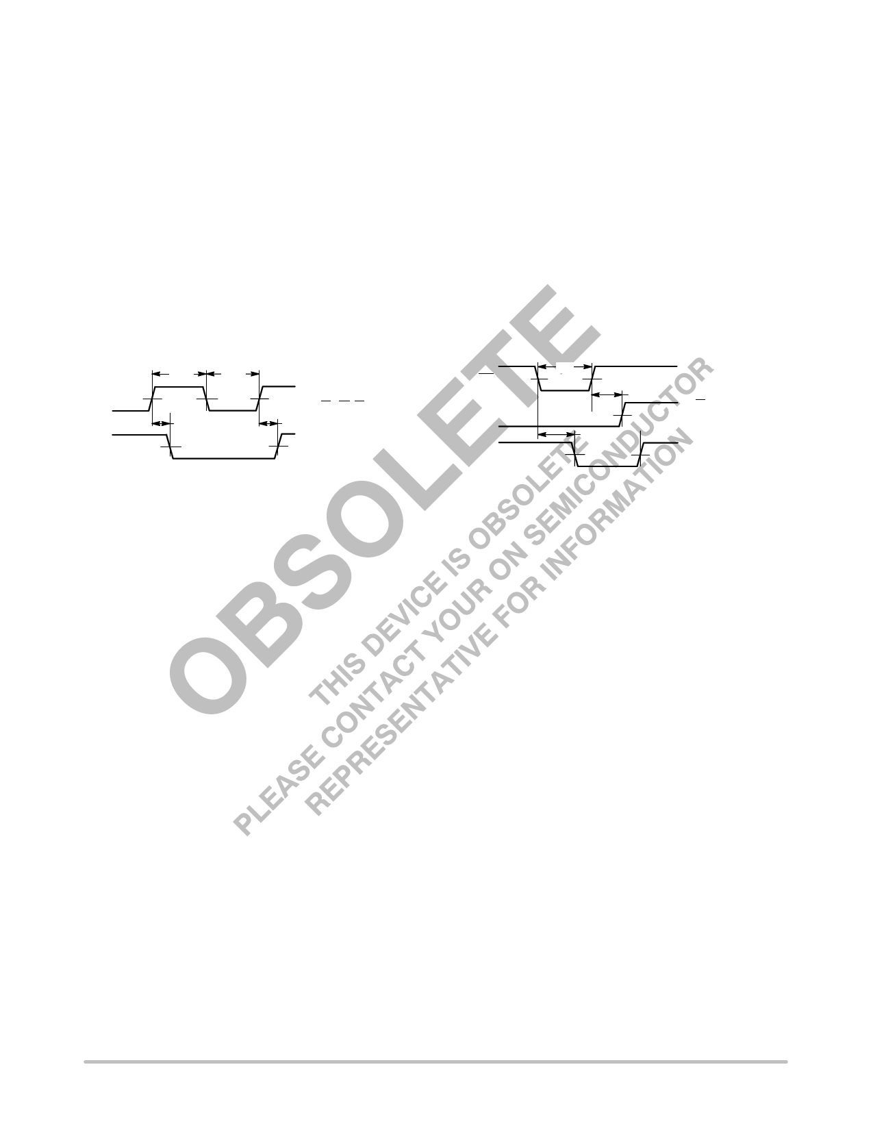
AC WAVEFORMS
tW(H)
tW(L)
CP
1.3 V
tPHL
1.3 V
tPLH
Other conditions:
PE = MR (SR) = H
CEP = CET = H
Q
1.3 V
1.3 V
MR 1.3 V
CP
Q0 V Q1 V Q2 V Q3
tW
tPHL
trec
1.3 V
Other conditions:
PE = L
P0 = P1 = P2 = P3 = H
1.3 V
Figure 1. Clock to Output Delays, Count Frequency, and Clock Pulse Width
Figure 2. Master Reset to Output Delay, Master Reset
Pulse Width, and Master Reset Recovery Time
http://onsemi.com
5
Share Link: 