NJU3553 データシートの表示(PDF) - Japan Radio Corporation
部品番号
コンポーネント説明
一致するリスト
NJU3553 Datasheet PDF : 17 Pages
| |||
NJU3553
2) Re-start signal Input Selection
PB0 terminal performs as the re-start terminal to return from “STANDBY” mode. It is selected by mask
option.
The STANDBY mode is released by the rising edge of the input signal to PB0 terminal, and the CPU re-
starts the execution from the last address before the STANDBY mode in.
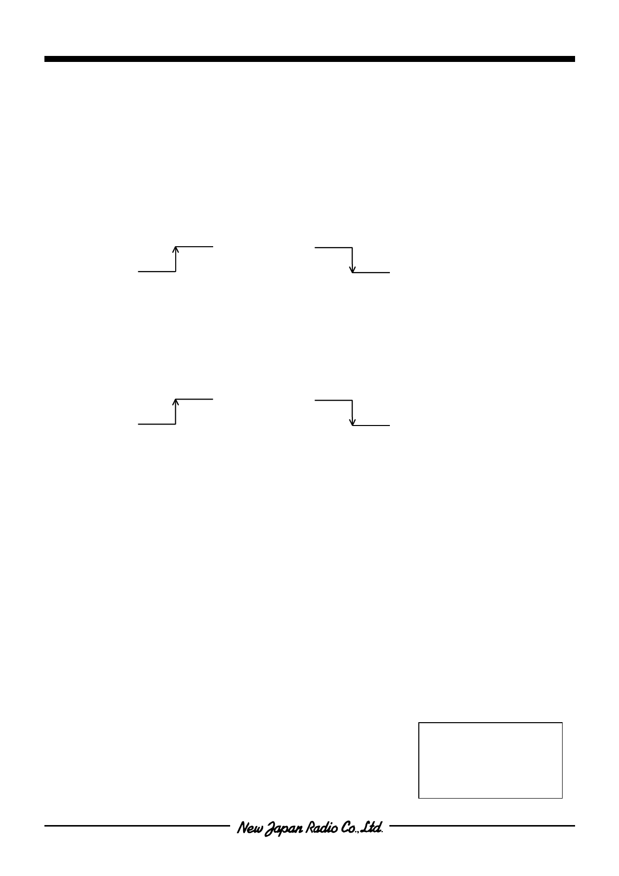
3) Edge Detector Selection
PB1 terminal is added the “Edge detect function” by the mask option.
Rising edge
Falling edge
4) External Interrupt of the edge Selection
When the interrupt function is set by mask option. PF0 terminal performs as the interrupt input
terminal. The polarity of the edge, rising as “low to high” or falling as “high to low”, is selected by the
mask option.
Rising edge
Falling edge
5) The data order (MSB, LSB) of the Serial Interface
The data order of the Serial Interface is selected select either MSB or LSB first by the mask option.
6) A/D Control Clock
A/D Control Clock is selected either the external clock from ADCK terminal or the internal clock from the
prescaler by the mask option.
7) Dividing ration of the internal clock
Each dividing ration of the count clocks of Timer1 and Timer2, the Internal shift clock of the Serial
Interface, the clock of the A/D control clock and the output clock through the SCK/CKOUT terminal is
selected among the following by the mask option.
The frequency of each clock is determined by the dividing ration and the 1-instruction term (1/fOSCx6).
1/2, 1/4, 1/8, 1/16, 1/32, 1/64, 1/128, 1/256, 1/512, 1/1024, 1/2048, 1/4096
Note) As Timer2 clock, the external clock or the internal is selected by the program.
As the shift clock of the serial interface, the external clock or the internal is selected by the program.
[CAUTION]
The specifications on this databook are only
given for information , without any guarantee
as regards either mistakes or omissions. The
application circuits in this databook are
described only to show representative usages
of the product and not intended for the
guarantee or permission of any right including
the industrial rights.
- 17 -
Share Link: 