CY7C4261V(2003) データシートの表示(PDF) - Cypress Semiconductor
部品番号
コンポーネント説明
一致するリスト
CY7C4261V Datasheet PDF : 16 Pages
| |||
CY7C4261V/CY7C4271V
CY7C4281V/CY7C4291V
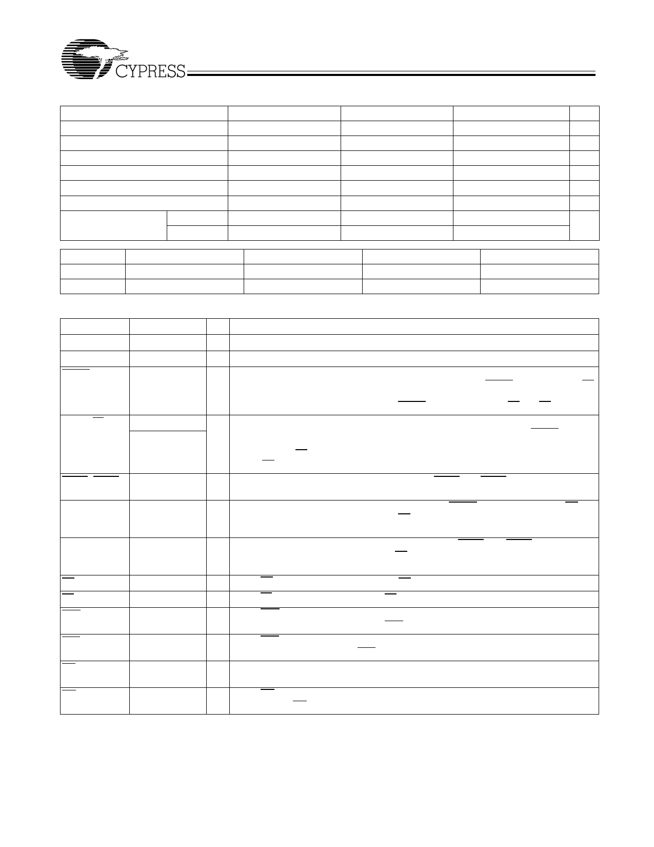
Selection Guide
Maximum Frequency
Maximum Access Time
Minimum Cycle Time
Minimum Data or Enable Set-up
Minimum Data or Enable Hold
Maximum Flag Delay
Active Power Supply
Current (ICC1)
Commercial
Industrial
7C4261/71/81/91V-10
100
8
10
3.5
0
8
25
7C4261/71/81/91V-15
66.7
10
15
4
0
10
25
30
7C4261/71/81/91V-25
40
15
25
6
1
15
25
Unit
MHz
ns
ns
ns
ns
ns
mA
Density
Package
CY7C4261V
16K x 9
32-pin PLCC
CY7C4271V
32K x 9
32-pin PLCC
CY7C4281V
64K x 9
32-pin PLCC
CY7C4291V
128K x 9
32-pin PLCC
Pin Definitions
Signal Name Description
D0−8
Q0−8
WEN1
Data Inputs
Data Outputs
Write Enable 1
WEN2/LD
Write Enable 2
Dual Mode Pin Load
REN1, REN2
WCLK
Read Enable
Inputs
Write Clock
RCLK
Read Clock
EF
Empty Flag
FF
Full Flag
PAE
Programmable
Almost Empty
PAF
Programmable
Almost Full
RS
Reset
OE
Output Enable
I/O
Description
I Data Inputs for 9-bit bus.
O Data Outputs for 9-bit bus.
I The only write enable when device is configured to have programmable flags.
Data is written on a LOW-to-HIGH transition of WCLK when WEN1 is asserted and FF is
HIGH. If the FIFO is configured to have two write enables, data is written on a LOW-to-HIGH
transition of WCLK when WEN1 is LOW and WEN2/LD and FF are HIGH.
I If HIGH at reset, this pin operates as a second write enable. If LOW at reset, this
pin operates as a control to write or read the programmable flag offsets. WEN1 must be
LOW and WEN2 must be HIGH to write data into the FIFO. Data will not be written into the FIFO
if the FF is LOW. If the FIFO is configured to have programmable flags, WEN2/LD is held LOW
to write or read the programmable flag offsets.
I Enables the device for Read operation. Both REN1 and REN2 must be asserted to
allow a read operation.
I The rising edge clocks data into the FIFO when WEN1 is LOW and WEN2/LD is HIGH
and the FIFO is not Full. When LD is asserted, WCLK writes data into the programmable
flag-offset register.
I The rising edge clocks data out of the FIFO when REN1 and REN2 are LOW and the
FIFO are not Empty. When WEN2/LD is LOW, RCLK reads data out of the programmable
flag-offset register.
O When EF is LOW, the FIFO is empty. EF is synchronized to RCLK.
O When FF is LOW, the FIFO is full. FF is synchronized to WCLK.
O When PAE is LOW, the FIFO is almost empty based on the almost empty offset value
programmed into the FIFO. PAE is synchronized to RCLK.
O When PAF is LOW, the FIFO is almost full based on the almost full offset value
programmed into the FIFO. PAF is synchronized to WCLK.
I Resets device to empty condition. A reset is required before an initial read or write
operation after power-up.
I When OE is LOW, the FIFO’s data outputs drive the bus to which they are connected. If
OE is HIGH, the FIFO’s outputs are in High Z (high-impedance) state.
Document #: 38-06013 Rev. *A
Page 2 of 16
Share Link: 