LM293 データシートの表示(PDF) - Philips Electronics
部品番号
コンポーネント説明
一致するリスト
LM293 Datasheet PDF : 6 Pages
| |||
Philips Semiconductors
Low power dual voltage comparator
Product specification
LM193/A/293/A/393/A/2903
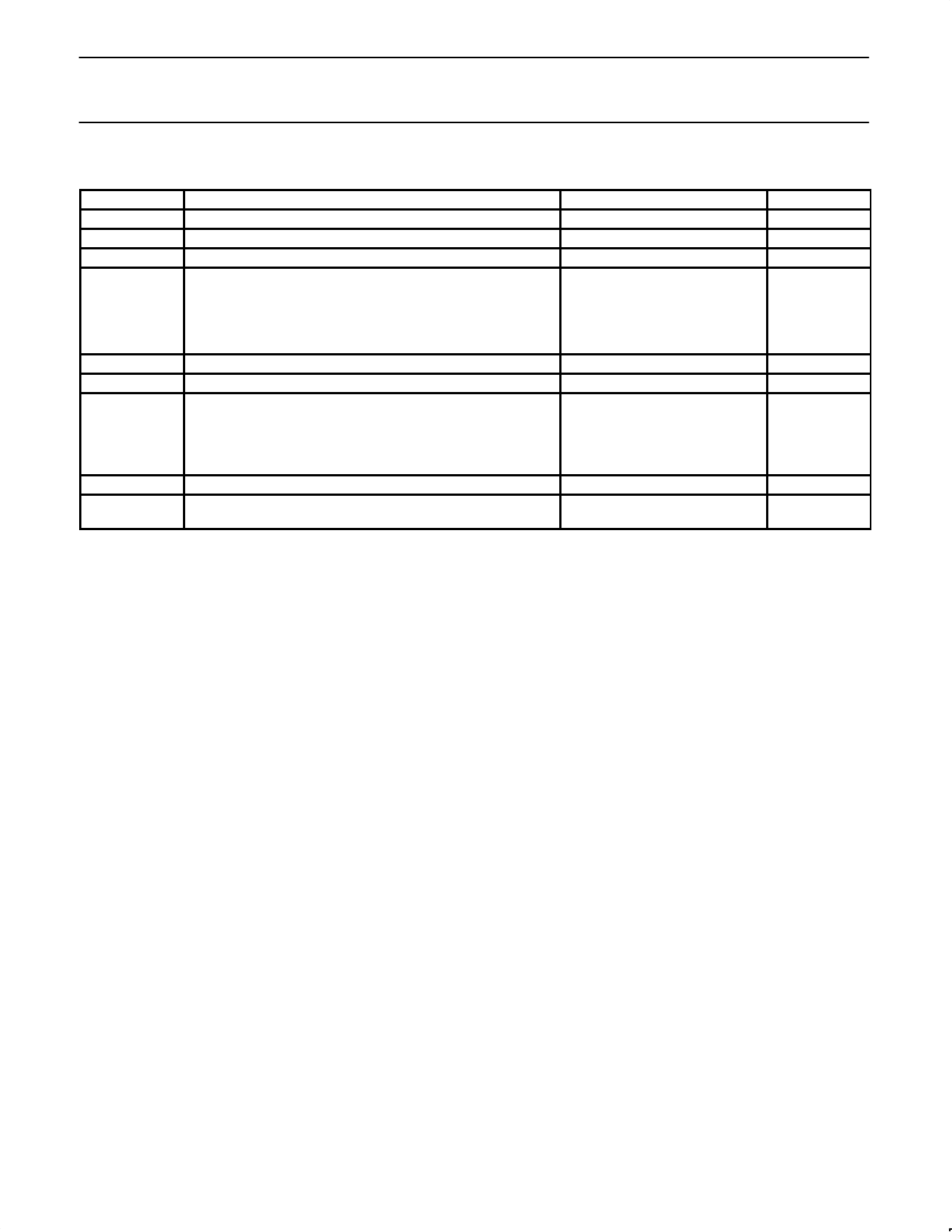
ABSOLUTE MAXIMUM RATINGS
SYMBOL
PARAMETER
VCC
Supply voltage
Differential input voltage
VIN
Input voltage
PD
Maximum power dissipation,
TA=25°C (still-air)1
F package
N package
D package
Output short-circuit to ground2
IIN
Input current (VIN<-0.3VDC)3
TA
Operating temperature range
LM193/193A
LM293/293A
LM393/393A
LM2903
TSTG
TSOLD
Storage temperature range
Lead soldering temperature
(10sec max)
RATING
36 or ±18
36
-0.3 to +36
780
1160
780
Continuous
50
-55 to +125
-25 to +85
0 to +70
-40 to +125
-65 to +150
300
UNIT
VDC
VDC
VDC
mW
mW
mW
mA
°C
°C
°C
°C
°C
°C
NOTES:
1. Derate above 25°C, at the following rates:
F package at 6.2mW/°C
N package at 9.3mW/°C
D package at 6.2mW/°C
2. Short circuits from the output to V+ can cause excessive heating and eventual destruction. The maximum output current is approximately
20mA independent of the magnitude of V+.
3. This input current will only exist when the voltage at any of the input leads is driven negative. It is due to the collector-base junction of the
input PNP transistors becoming forward biased and thereby acting as input diode clamps. In addition to this diode action, there is also lateral
NPN parasitic transistor action on the IC chip. This transistor action can cause the output voltages of the comparators to go to the V+ voltage
level (or to ground for a large overdrive) for the time duration that an input is driven negative. This is not destructive and normal output states
will re-establish when the input voltage, which was negative, again returns to a value greater than -0.3VDC.
1995 Nov 27
2
Share Link: 