MC74HC365A データシートの表示(PDF) - Motorola => Freescale
部品番号
コンポーネント説明
一致するリスト
MC74HC365A Datasheet PDF : 6 Pages
| |||
MOTOROLA
SEMICONDUCTOR TECHNICAL DATA
Advance Information
Hex 3-State Noninverting
Buffer with Common Enables
High–Performance Silicon–Gate CMOS
The MC74HC365A is identical in pinout to the LS365. The device inputs
are compatible with standard CMOS outputs; with pullup resistors, they are
compatible with LSTTL outputs.
This device is a high–speed hex buffer with 3–state outputs and two
common active–low Output Enables. When either of the enables is high, the
buffer outputs are placed into high–impedance states. The HC365A has
noninverting outputs.
• Output Drive Capability: 15 LSTTL Loads
• Outputs Directly Interface to CMOS, NMOS, and TTL
• Operating Voltage Range: 2 to 6 V
• Low Input Current: 1 µA
• High Noise Immunity Characteristic of CMOS Devices
• In Compliance with the Requirements Defined by JEDEC Standard
No. 7A
• Chip Complexity: 90 FETs or 22.5 Equivalent Gates
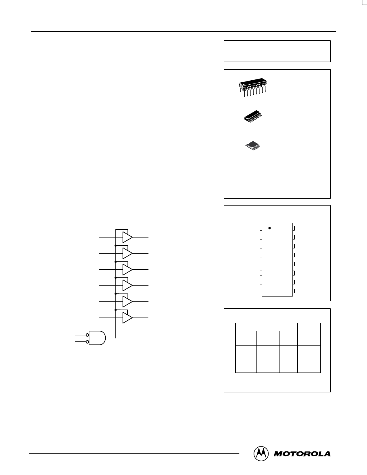
LOGIC DIAGRAM
A0 2
A1 4
A2 6
A3 10
A4 12
A5 14
OUTPUT ENABLE 1 1
OUTPUT ENABLE 2 15
3 Y0
5 Y1
7 Y2
9 Y3
11 Y4
13 Y5
PIN 16 = VCC
PIN 8 = GND
MC74HC365A
N SUFFIX
PLASTIC PACKAGE
16–LEAD
CASE 648–08
D SUFFIX
SOIC PACKAGE
16–LEAD
CASE 751B–05
DT SUFFIX
TSSOP PACKAGE
16–LEAD
CASE 948F–01
ORDERING INFORMATION
MC74HCXXXAN
MC74HCXXXAD
MC74HCXXXADT
Plastic
SOIC
TSSOP
PIN ASSIGNMENT
OUTPUT
ENABLE 1
1
A0 2
Y0 3
16 VCC
15
OUTPUT
ENABLE 2
14 A5
A1 4
13 Y5
Y1 5
12 A4
A2 6
11 Y4
Y2 7
10 A3
GND 8
9 Y3
FUNCTION TABLE
Inputs
Output
Enable Enable
1
2
A
Y
L
L
L
L
L
L
H
H
H
X
X
Z
X
H
X
Z
X = don’t care
Z = high impedance
This document contains information on a new product. Specifications and information herein are subject to
change without notice.
3/97
© Motorola, Inc. 1997
1
REV 0.1
Share Link: 