8405202XA データシートの表示(PDF) - Intersil
部品番号
コンポーネント説明
一致するリスト
8405202XA Datasheet PDF : 35 Pages
| |||
80C86
devices. The read control signal is also asserted at T2. The
read (RD) signal causes the addressed device to enable its
data bus drivers to the local bus. Some time later, valid data
will be available on the bus and the addressed device will
drive the READY line HIGH. When the processor returns the
read signal to a HIGH level, the addressed device will again
three-state its bus drivers. If a transceiver (82C86/82C87) is
required to buffer the 80C86 local bus, signals DT/R and
DEN are provided by the 80C86.
A write cycle also begins with the assertion of ALE and the
emission of the address. The M/IO signal is again asserted
to indicate a memory or I/O write operation. In T2, immedi-
ately following the address emission, the processor emits
the data to be written into the addressed location. This data
remains valid until at least the middle of T4. During T2, T3
and TW, the processor asserts the write control signal. The
write (WR) signal becomes active at the beginning of T2 as
opposed to the read which is delayed somewhat into T2 to
provide time for output drivers to become inactive.
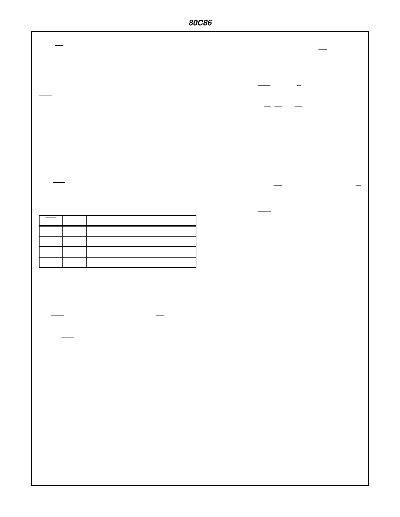
The BHE and A0 signals are used to select the proper
byte(s) of the memory/lO word to be read or written accord-
ing to Table 5.
TABLE 5.
BHE
A0
CHARACTERISTICS
0
0 Whole word
0
1 Upper Byte From/To Odd Address
1
0 Lower Byte From/To Even Address
1
1 None
Bus Timing - Medium Size Systems
For medium complexity systems the MN/MX pin is con-
nected to GND and the 82C88 Bus Controller is added to the
system as well as an 82C82/82C83 latch for latching the
system address, and an 82C86/82C87 transceiver to allow
for bus loading greater than the 80C86 is capable of han-
dling. Signals ALE, DEN, and DT/R are generated by the
82C88 instead of the processor in this configuration,
although their timing remains relatively the same. The
80C86 status outputs (S2, S1 and S0) provide type-of-cycle
information and become 82C88 inputs. This bus cycle infor-
mation specifies read (code, data or I/O), write (data or I/O),
interrupt acknowledge, or software halt. The 82C88 issues
control signals specifying memory read or write, I/O read or
write, or interrupt acknowledge. The 82C88 provides two
types of write strobes, normal and advanced, to be applied
as required. The normal write strobes have data valid at the
leading edge of write. The advanced write strobes have the
same timing as read strobes, and hence, data is not valid at
the leading edge of write. The 82C86/82C87 transceiver
receives the usual T and OE inputs from the 82C88 DT/R
and DEN signals.
The pointer into the interrupt vector table, which is passed
during the second INTA cycle, can be derived from an
82C59A located on either the local bus or the system bus. If
the master 82C59A Priority Interrupt Controller is positioned
on the local bus, the 82C86/82C87 transceiver must be dis-
abled when reading from the master 82C59A during the
interrupt acknowledge sequence and software “poll”.
I/O ports are addressed in the same manner as memory
location. Even addressed bytes are transferred on the D7-D0
bus lines and odd address bytes on D15-D8.
The basic difference between the interrupt acknowledge
cycle and a read cycle is that the interrupt acknowledge sig-
nal (INTA) is asserted in place of the read (RD) signal and
the address bus is held at the last valid logic state by internal
bus hold devices. (See Figure 4). In the second of two suc-
cessive INTA cycles a byte of information is read from the
data bus (D7-D0) as supplied by the interrupt system logic
(i.e., 82C59A Priority Interrupt Controller). This byte identi-
fies the source (type) of the interrupt. It is multiplied by four
and used as a pointer into an interrupt vector lookup table,
as described earlier.
3-154
Share Link: 