LT1175-5 データシートの表示(PDF) - Linear Technology
部品番号
コンポーネント説明
一致するリスト
LT1175-5 Datasheet PDF : 38 Pages
| |||
LTC1966
Applications Information
How an RMS-to-DC Converter Works
Monolithic RMS-to-DC converters use an implicit com-
putation to calculate the RMS value of an input signal.
The fundamental building block is an analog multiply/
divide used as shown in Figure 3. Analysis of this topol-
ogy is easy and starts by identifying the inputs and the
output of the lowpass filter. The input to the LPF is the
calculation from the multiplier/divider; (VIN)2/VOUT. The
lowpass filter will take the average of this to create the
output, mathematically:
VOUT
=
(VIN)2
VOUT
,
Because VOUT is DC,
(VIN)2
VOUT
=
(
VIN)2
VOUT
,
so
VOUT
=
(VIN
)2
VOUT
,
and
(VOUT)2 = (VIN)2, or
VOUT = (VIN)2 = RMS(VIN)
( )VIN 2
VOUT
VIN
×÷
LPF
VOUT
1966 F03
Figure 3. RMS-to-DC Converter with Implicit Computation
Unlike the prior generation RMS-to-DC converters, the
LTC1966 computation does NOT use log/antilog circuits,
which have all the same problems, and more, of log/antilog
multipliers/dividers, i.e., linearity is poor, the bandwidth
changes with the signal amplitude and the gain drifts with
temperature.
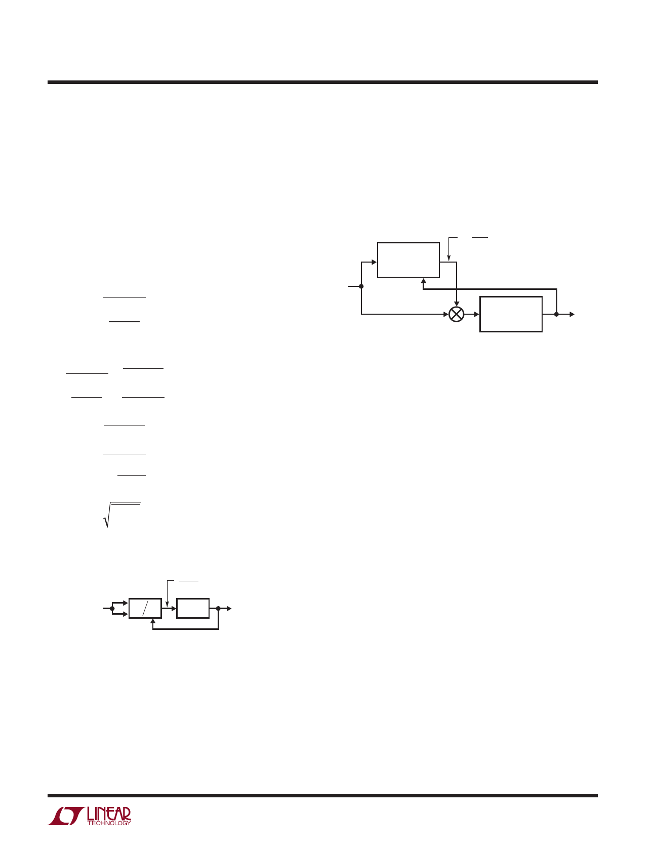
How the LTC1966 RMS-to-DC Converter Works
The LTC1966 uses a completely new topology for RMS-
to-DC conversion, in which a ∆Σ modulator acts as the
divider, and a simple polarity switch is used as the multiplier
as shown in Figure 4.
∆–∑
REF
D α VIN
VOUT
VIN
±1
LPF
VOUT
Figure 4. Topology of LTC1966
The ∆Σ modulator has a single-bit output whose average
duty cycle (D) will be proportional to the ratio of the input
signal divided by the output. The ∆Σ is a 2nd order modula-
tor with excellent linearity. The single bit output is used to
selectively buffer or invert the input signal. Again, this is a
circuit with excellent linearity, because it operates at only
two points: ±1 gain; the average effective multiplication
over time will be on the straight line between these two
points. The combination of these two elements again creates
a lowpass filter input signal proportional to (VIN)2/VOUT,
which, as shown above, results in RMS-to-DC conversion.
The lowpass filter performs the averaging of the RMS
function and must be a lower corner frequency than the
lowest frequency of interest. For line frequency measure-
ments, this filter is simply too large to implement on-chip,
but the LTC1966 needs only one capacitor on the output
to implement the lowpass filter. The user can select this
capacitor depending on frequency range and settling time
requirements, as will be covered in the Design Cookbook
section to follow.
This topology is inherently more stable and linear than
log/antilog implementations primarily because all of the
signal processing occurs in circuits with high gain op amps
operating closed loop.
1966fb
11
Share Link: 