AS6C6264A データシートの表示(PDF) - Alliance Semiconductor
部品番号
コンポーネント説明
一致するリスト
AS6C6264A Datasheet PDF : 10 Pages
| |||
MARCH 2009
AS6C6264A
8K X 8 BIT LOW POWER CMOS SRAM
FEATURES
8192 x 8 bit static CMOS RAM
70 ns Access Times
Common data inputs and
outputs
Three-state outputs
Typ. operating supply current
o 70 ns: 10 mA
Standby current:
o < 2 μA at Ta ≤ 70 °C
Data retention current at 2 V:
o < 1 μA at Ta ≤ 70 °C
TTL/CMOS-compatible
Automatic reduction of power
dissipation in long Read or Write
cycles
Power supply voltage 5 V
Operating temperature ranges:
o 0 to 70 °C
o -40 to 85 °C
ESD protection > 2000 V
(MIL STD 883C M3015.7)
Latch-up immunity > 100 mA
Packages: PDIP28 (600 mil)
SOP28 (330 mil)
DESCRIPTION
The AS6C6264A is a static RAM
manufactured using a CMOS
process technology with the
following operating modes:
- Read - Standby
- Write - Data Retention
The memory array is based on a 6-
transistor cell.
The circuit is activated by the rising
edge of E2 (at E1 = L), or the falling
edge of E1 (at E2 = H). The address
and control inputs open
simultaneously. According to the
information of W and G, the data
inputs, or outputs, are active. In a
Read cycle, the data outputs are
activated by the falling edge of G,
afterwards the data word read will
be available at the outputs DQ0 -
DQ7. After the address change, the
data outputs go High-Z until the new
read information is available. The
data outputs have no preferred
state. If the memory is driven by
CMOS levels in the active state, and
if there is no change of the address,
data input and control signals W or
G, the operating current (at IO = 0
mA) drops to the value of the
operating current in the Standby
mode. The Read cycle is finished by
the falling edge of E2 or W, or by
the rising edge of E1, respectively.
Data retention is guaranteed down
to 2 V. With the exception of E2, all
inputs consist of NOR gates, so that
no pull-up/pull-down resistors are
required. This gate circuit allows to
achieve low power standby
requirements by activation with TTL-
levels too.
If the circuit is inactivated by E2 = L,
the standby current
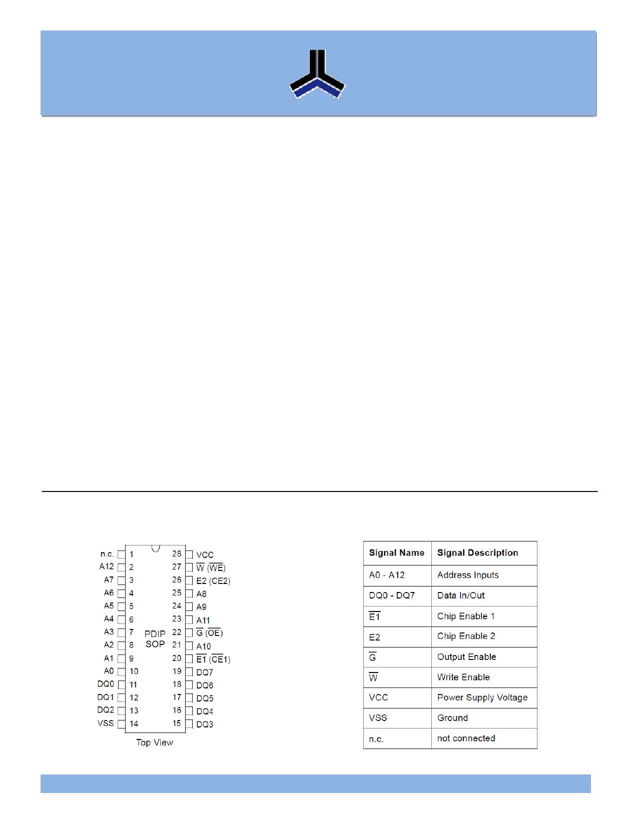
PIN CONFIGURATION
PIN DESCRIPTION
MARCH/2009
ALLIANCE MEMORY
PAGE 1 of 10
Share Link: 