CXA2074Q/S データシートの表示(PDF) - Sony Semiconductor
部品番号
コンポーネント説明
一致するリスト
CXA2074Q/S Datasheet PDF : 38 Pages
| |||
Pin Description
Pin No.
QFP SDIP
Symbol
Pin
voltage
44 1 BASSR1 4.0V
(45) 2
45 2 BASSR2 4.0V (47) 4
46 3 BASSL1 4.0V
47 4 BASSL2 4.0V
CXA2074Q/S
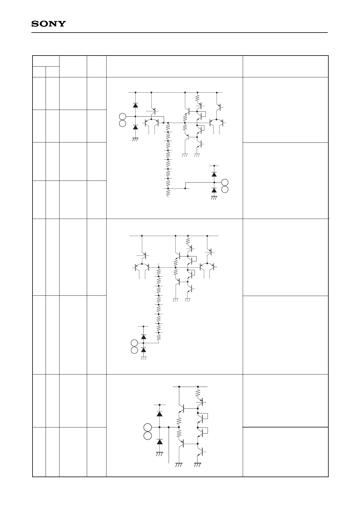
Equivalent circuit
3k
190
4.2k 190
3.4k
2.7k
2.2k
1.8k
1.4k
1.2k
4.9k
4V
Description
BASS filter pin. (Right channel)
VCC
(Connect a 47nF capacitor
between Pins 1 and 2 (44
and 45).)
The cutoff frequency is
determined by the built-in
resistor and the external
capacitance.
VCC
1 (44)
3 (46)
BASS filter pin. (Left channel)
(Connect a 47nF capacitor
between Pins 3 and 4 (46
and 47).)
The cutoff frequency is
determined by the built-in
resistor and the external
capacitance.
48 5 TRER 4.0V
1 6 TREL 4.0V
VCC
(48) 5
(1) 6
3k
580
4.2k 580
3.4k
2.7k
2.2k
1.8k
1.4k
1.2k
4.9k
VCC
TREBLE filter pin.
(Right channel)
(Connect a 6.8nF capacitor
between this pin and GND.)
TREBLE filter pin.
(Left channel)
(Connect a 6.8nF capacitor
between this pin and GND.)
2 7 LSOUT-R 4.0V
3 8 LSOUT-L 4.0V
VCC
3k
VCC
580
(2) 7
(3) 8
580
–5–
LSOUT right channel output
pin.
LSOUT left channel output
pin.
Share Link: 