UPD720100A データシートの表示(PDF) - NEC => Renesas Technology
部品番号
コンポーネント説明
一致するリスト
UPD720100A Datasheet PDF : 32 Pages
| |||
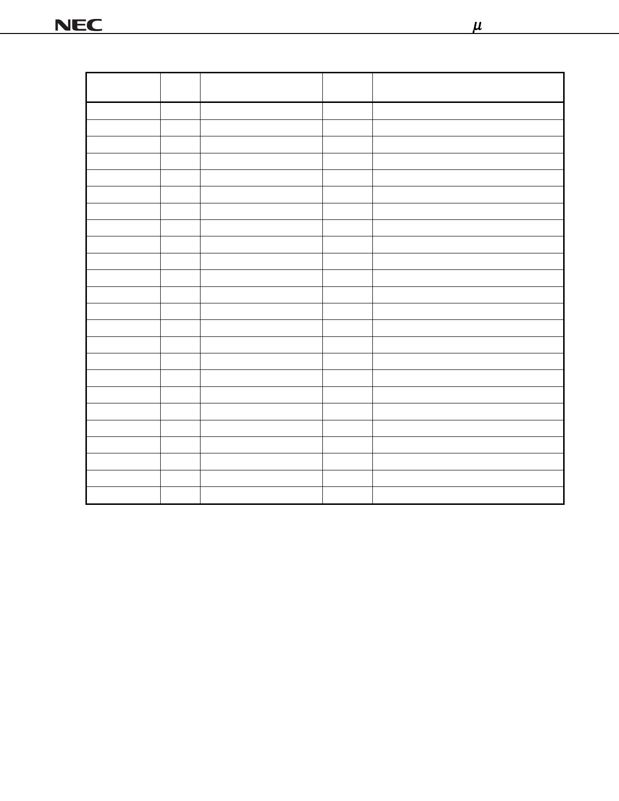
µPD720100A
Pin Name
I/O
Buffer Type
Active
Level
Function
(2/2)
RREF
A
Analog
Reference resistor
PC1
A
Analog
Capacitor for PLL
PC2
A
Analog
Capacitor for PLL
NTEST(2:1)
I
Input with 12 kΩ Pull down R High
Test pin
SMC
I
Input with 50 kΩ Pull down R High
Scan mode control
SIN/TIN
I
Input with 50 kΩ Pull down R
Scan input or RAM BIST input
SOT/TOUT
O
Output
Scan output or RAM BIST output
TEB
I
Input with 50 kΩ Pull down R High
BIST enable
AMC
I
Input with 50 kΩ Pull down R High
ATG mode control
SCK/TCLK
I
Input with 50 kΩ Pull down R
Scan clock or RAM BIST clock
CLKSEL
I
Input with 50 kΩ Pull down R
Clock select signal
TEST
I
Input with 50 kΩ Pull down R High
Test Control
NANDTEST
I
Input with 50 kΩ Pull down R High
NAND Tree Test enable
SELDAT
O
Output
Test signal
SELCLK
O
Output
Test signal
SRCLK
O
Output
Serial ROM Clock Out
SRDTA
I/O
I/O
Serial ROM Data
SRMOD
I
Input with 50 kΩ Pull down R High
Serial ROM Input Enable
AVDD
VDD for Analog circuit
VDD
VDD
VDD_PCI
5 V (5 V PCI) or 3.3 V (3.3 V PCI)
AVSS
VSS for Analog circuit
VSS
VSS
N.C.
Not connect
Remarks 1. “5 V tolerant“ means that the buffer is 3 V buffer with 5 V tolerant circuit.
2. “5 V PCI” indicates a PCI buffer, which complies with the 3 V PCI standard, has a 5 V tolerant circuit.
It does not indicate a buffer that fully complies with 5 V PCI standard. However, this function can be
used for evaluating the operation of a device on a 5V add-in card.
3. The signal marked as “(I/O)” in the above table operates as I/O signals during testing. However, they
do not need to be considered in normal use.
Data Sheet S15535EJ2V0DS
9
Share Link: 