R5F21331CDFP データシートの表示(PDF) - Renesas Electronics
部品番号
コンポーネント説明
一致するリスト
R5F21331CDFP Datasheet PDF : 56 Pages
| |||
R8C/33C Group
1. Overview
1.5 Pin Functions
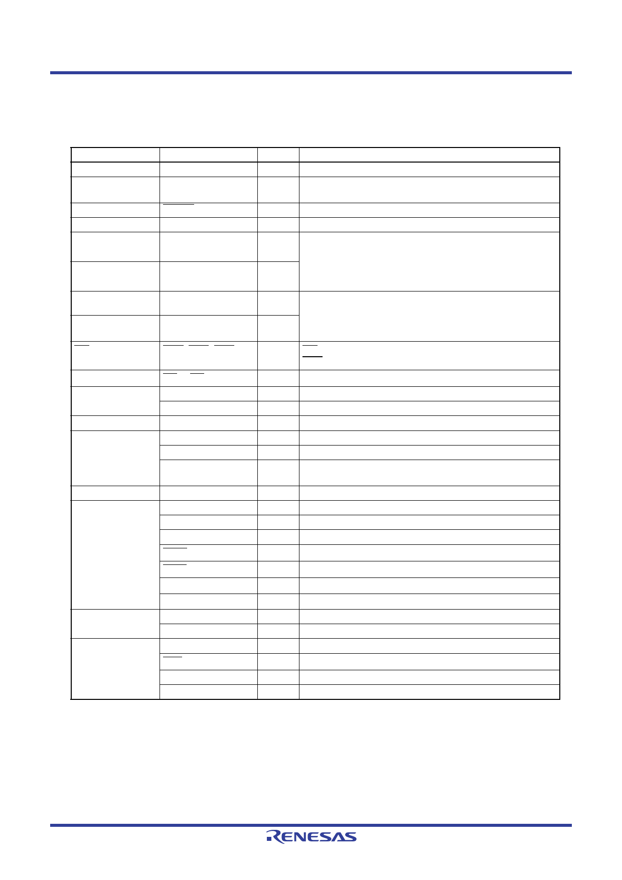
Tables 1.5 and 1.6 list Pin Functions.
Table 1.5 Pin Functions (1)
Item
Power supply input
Analog power
supply input
Reset input
MODE
XIN clock input
Pin Name
VCC, VSS
AVCC, AVSS
RESET
MODE
XIN
XIN clock output XOUT
I/O Type
Description
− Apply 1.8 V to 5.5 V to the VCC pin. Apply 0 V to the VSS pin.
− Power supply for the A/D converter.
Connect a capacitor between AVCC and AVSS.
I Input “L” on this pin resets the MCU.
I Connect this pin to VCC via a resistor.
I These pins are provided for XIN clock generation circuit I/O.
Connect a ceramic resonator or a crystal oscillator between
I/O
the XIN and XOUT pins (1). To use an external clock, input it
to the XOUT pin and leave the XIN pin open.
XCIN clock input XCIN
XCIN clock output XCOUT
I These pins are provided for XCIN clock generation circuit I/O.
Connect a crystal oscillator between the XCIN and XCOUT
O pins (1). To use an external clock, input it to the XCIN pin and
leave the XCOUT pin open.
INT interrupt input INT0, INT1, INT3
Key input interrupt
Timer RA
Timer RB
Timer RC
Timer RE
Serial interface
I2C bus
SSU
KI0 to KI3
TRAIO
TRAO
TRBO
TRCCLK
TRCTRG
TRCIOA, TRCIOB,
TRCIOC, TRCIOD
TREO
CLK0, CLK1, CLK2
RXD0, RXD1, RXD2
TXD0, TXD1, TXD2
CTS2
RTS2
SCL2
SDA2
SCL
SDA
SSI
SCS
SSCK
SSO
I INT interrupt input pins.
INT0 is timer RB, and RC input pin.
I Key input interrupt input pins
I/O Timer RA I/O pin
O Timer RA output pin
O Timer RB output pin
I External clock input pin
I External trigger input pin
I/O Timer RC I/O pins
O Divided clock output pin
I/O Transfer clock I/O pins
I Serial data input pins
O Serial data output pins
I Transmission control input pin
O Reception control output pin
I/O I2C mode clock I/O pin
I/O I2C mode data I/O pin
I/O Clock I/O pin
I/O Data I/O pin
I/O Data I/O pin
I/O Chip-select signal I/O pin
I/O Clock I/O pin
I/O Data I/O pin
I: Input
O: Output
I/O: Input and output
Note:
1. Refer to the oscillator manufacturer for oscillation characteristics.
R01DS0008EJ0100 Rev 1.00
Aug. 24, 2010
Page 8 of 53
Share Link: 