LC72323 データシートの表示(PDF) - SANYO -> Panasonic
部品番号
コンポーネント説明
一致するリスト
LC72323 Datasheet PDF : 13 Pages
| |||
Pin Functions
Pin
Pin No.
LC72323
Function
I/O
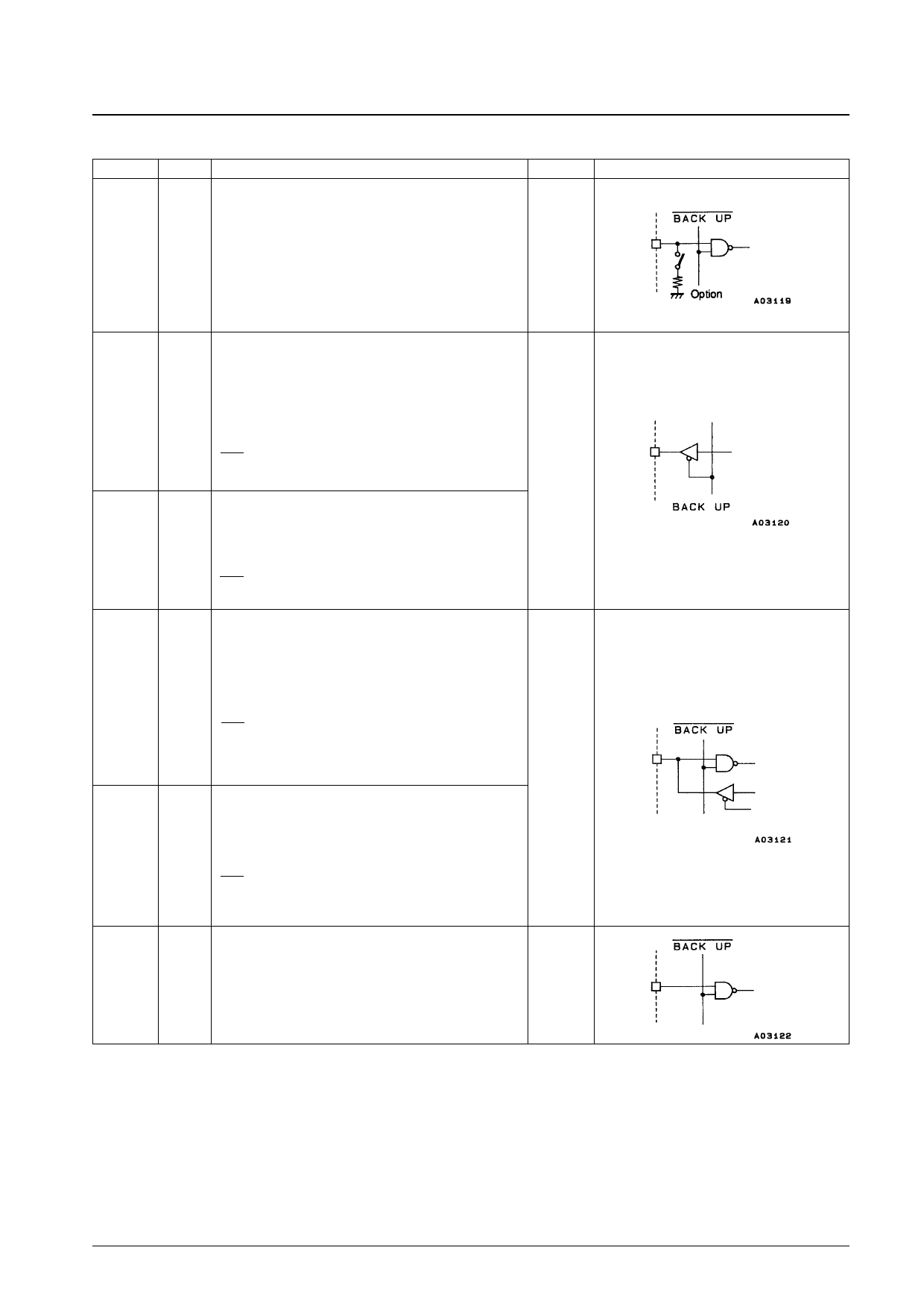
Low-threshold type dedicated input port
PA0
35
These pins can be used, for example, for key data acquisition.
PA1
34
Built-in pull-down resistors can be specified as an option. This
Input
PA2
33
option is in 4-pin units, and cannot be specified for individual
PA3
32
pins.
Input through these pins is disabled in BACKUP mode.
PB0
30
PB1
29
Dedicated output ports
PB2
28
Since the output transistor impedances are unbalanced
PB3
27
CMOS, these pins can be effectively used for functions such
as key scan timing. These pins go to the output high-
PC0
26
impedance state in BACKUP mode.
PC1
25
These pins go to the low level during a reset, i.e., when the
PC2
24
RES pin is low.
PC3
23
Output
PD0
22
Dedicated output ports
PD1
21
These are normal CMOS outputs. These pins go to the output
high-impedance state in BACKUP mode.
PD2
20
These pins go to the low level during a reset, i.e., when the
PD3
19
RES pin is low.
PE0
PE1
PE2
PE3
PF0
PF1
PF2
PF3
PG0
PG1
PG2
PG3
I/O port
These pins are switched between input and output as follows:
18
Once an input instruction (IN, TPT, or TPF) is executed, these
17
pins latch in the input mode. Once an output instruction (OUT,
SPB, or RPB) is executed, they latch in the output mode.
16
These pins go to the input mode during a reset, i.e., when the
15
RES pin is low.
In BACKUP mode these pins go to the input mode with input
disabled.
I/O
I/O port
These pins are switched between input and output by the
14
FPC instruction.
13
The I/O states of this port can be specified for individual pins.
12
These pins go to the input mode during a reset, i.e., when the
11
RES pin is low.
In BACKUP mode these pins go to the input mode with input
disabled.
6
5
Dedicated input port
4
Input through these pins is disabled in BACKUP mode.
3
Input
I/O circuit type
Continued on next page.
No. 4950-7/13
Share Link: 