IMSC011 データシートの表示(PDF) - STMicroelectronics
部品番号
コンポーネント説明
一致するリスト
IMSC011 Datasheet PDF : 30 Pages
| |||
3 System services
the device. If ClockIn is gated to achieve this, its skew must be limited to the value TDCHSIQH shown
in table 3.3. The mode of operation (Mode 1, Mode 2) must not be changed dynamically.
SeparateIQ
VDD
ClockIn
GND
Mode
1
1
2
Link Speed Mbits/sec
10
20
10 or 20
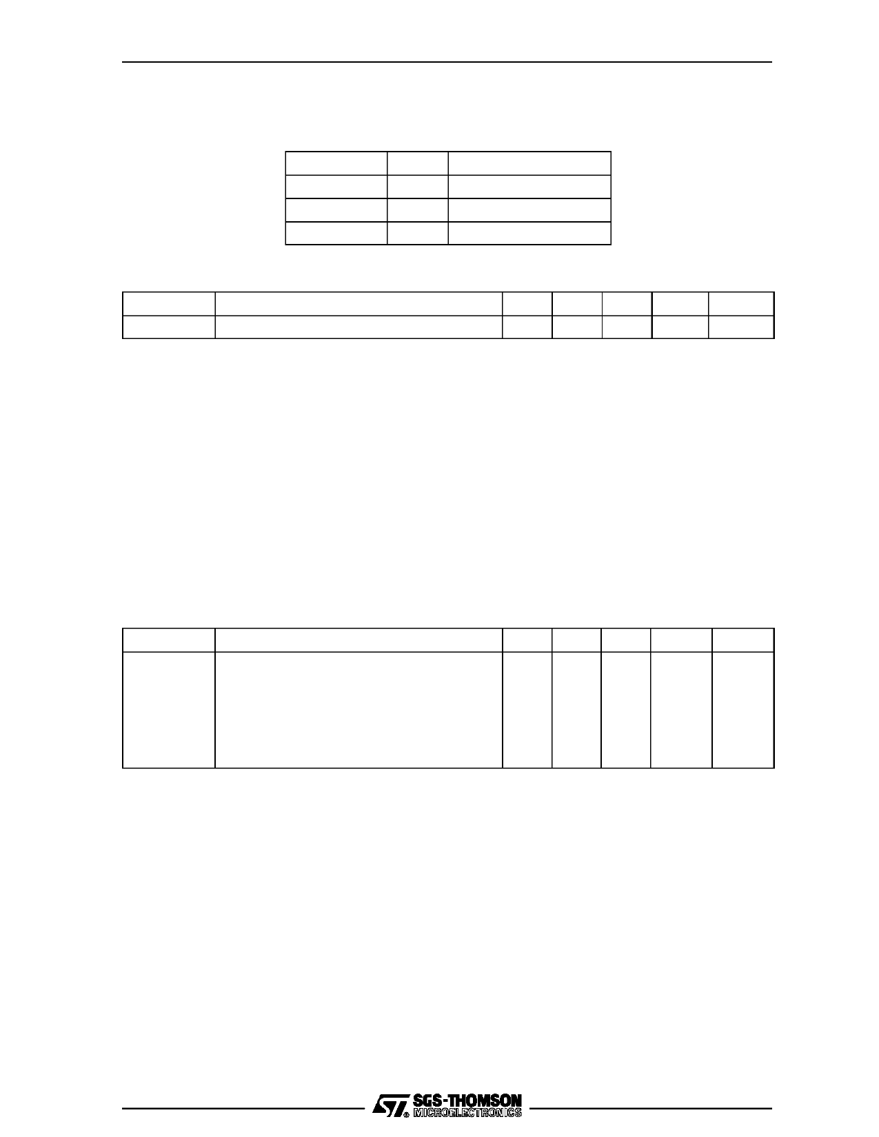
Table 3.2 SeparateIQ mode selection
Symbol
Parameter
TDCHSIQH Skew from ClockIn to ClockIn
Min Nom Max Units Notes
20 ns
1
Notes
1 Skew between ClockIn arriving on the ClockIn pin and on the SeparateIQ pin.
Table 3.3 SeparateIQ
3.5 Reset
The Reset pin can go high with VDD, but must at no time exceed the maximum specified voltage for VIH.
After VDD is valid ClockIn should be running for a minimum period TDCVRL before the end of Reset. All
inputs, with the exception of ClockIn and SeparateIQ (plus LinkSpeed in mode 2), must be held in their
inactive state during reset.
Reset initialises the IMS C011 to the following state: LinkOut is held low; the control outputs (IAck and
QValid in Mode 1, InputInt and OutputInt in Mode 2) are held low; interrupts (Mode 2) are disabled; the
states of Q0-7 in Mode 1 are unspecified; D0-7 in Mode 2 are high impedance.
Symbol
TPVRH
TRHRL
TDCVRL
TRLIvH
TRLCSL
Parameter
Power valid before Reset
Reset pulse width high
ClockIn running before Reset end
Reset low before IValid high (mode 1)
Reset low before chip select low (mode 2)
Min Nom Max
10
8
10
0
0
Units
ms
ClockIn
ms
ns
ns
Notes
1
2
Notes
1 Full periods of ClockIn TDCLDCL required.
2 At power-on reset.
Table 3.4 Reset
7 / 30
Share Link: 