FXAS21002CQR1 データシートの表示(PDF) - Freescale Semiconductor
部品番号
コンポーネント説明
一致するリスト
FXAS21002CQR1 Datasheet PDF : 58 Pages
| |||
Digital Interfaces
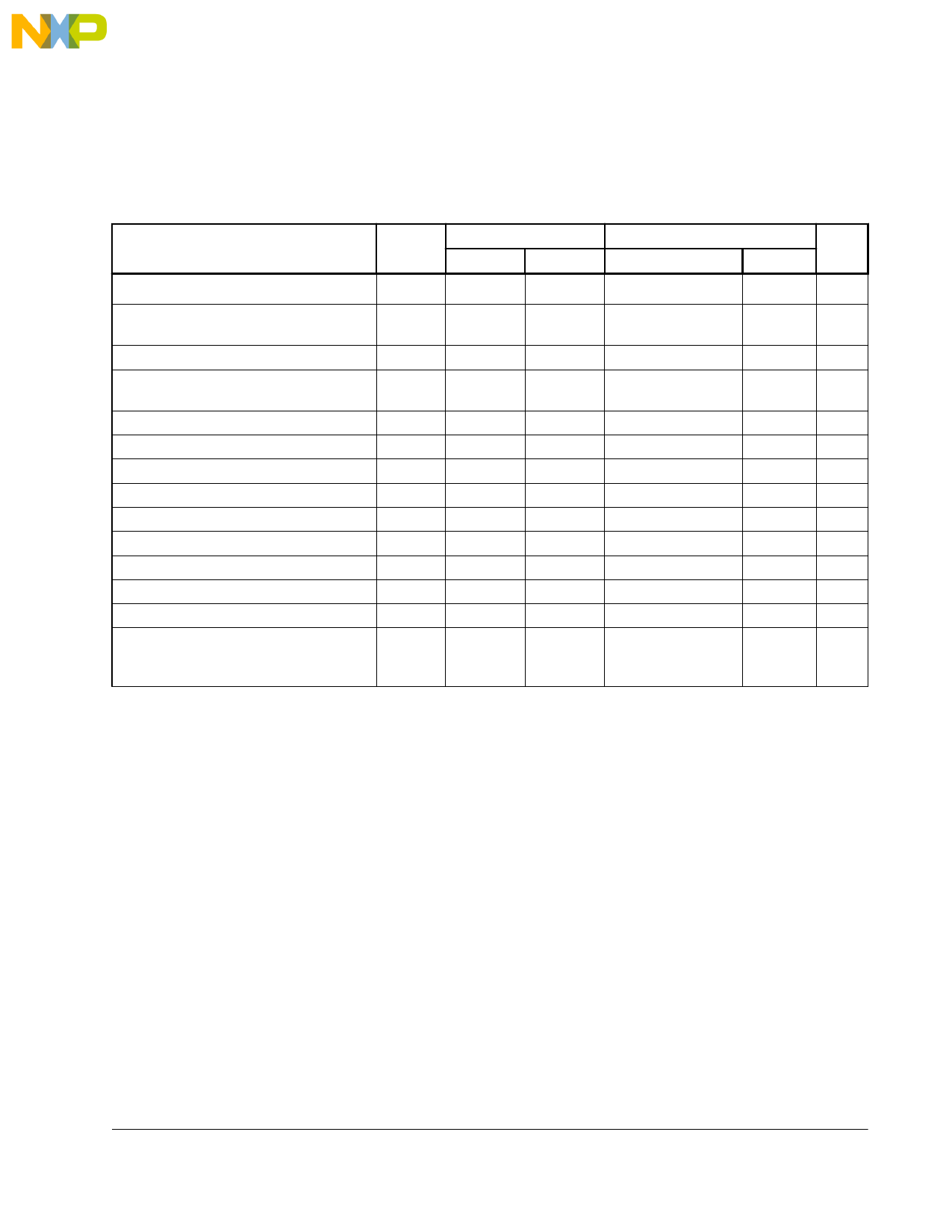
The key bus timing constraints are shown in Table 10. The I2C timing diagram is
shown in Figure 6.
Table 10. Slave timing values
Parameter
Symbol I2C Standard Mode1, 2
Min
Max
I2C Fast Mode1, 2
Min
Max
Unit
SCL clock frequency
Bus free time between STOP and
START conditions
fSCL
0
tBUF
4.7
Hold time (repeated) START condition
tHD;STA
4.0
Set-up time for a repeated START
condition
tSU;STA
4.7
Set-up time for a STOP condition
tSU;STO
4.0
SDA valid time2
tVD;DAT
—
SDA valid acknowledge time4
tVD;ACK
—
SDA setup time
tSU;DAT
250
SCL clock low time
tLOW
4.7
SCL clock high time
tHIGH
4.0
SDA and SCL rise time
tr
—
SDA and SCL fall time6
tf
—
Capacitive load for each bus line7
Cb
—
Pulse width of spikes on SDA and SCL
that must be suppressed by the internal
tSP
0
input filter
100
—
—
—
—
3.453
3.453
—
—
—
1000
300
400
50
0
1.3
0.6
0.6
0.6
—
—
1005
1.3
0.6
20
20*(VDDIO/5.5 V)
—
0
400
kHz
—
µs
—
µs
—
µs
—
µs
0.93
µs
0.93
µs
—
ns
—
µs
—
µs
300
ns
300
ns
400
pF
50
ns
1. All values refer to VIH (min) and VIL (max) levels.
2. tVD;DAT refers to the time for data signal from SCL LOW to SDA output (HIGH or LOW, depending on which one is
worse).
3. The maximum tHD;DAT could be 3.45 µs and 0.9 µs for Standard mode and Fast mode, but must be less than the
maximum of tVD;DAT or tVD;ACK by a transition time.
4. tVD;ACK = time for acknowledgement signal from SCL LOW to SDA output (HIGH or LOW, depending on which one is
worse).
5. A Fast-mode I2C device can be used in a Standard-mode I2C system, but the requirement tSU;DAT 250 ns must then
be met. Also, the acknowledge timing must meet this set-up time.
6. The maximum tf for the SDA and SCL bus lines is specified at 300 ns. The maximum fall time for the SDA output
stage tf is specified at 250 ns. This allows series protection resistors to be connected between the SDA and the SCL
pins and the SDA/SCL bus lines without exceeding the maximum specified tf.
7. Cb is the total capacitance of one bus line in pF; the maximum bus capacitance allowable may vary from this value
depending on the application operating voltage and frequency.
3-Axis Digital Angular Rate Gyroscope, Rev. 2.1, 5/2015
13
Freescale Semiconductor, Inc.
Share Link: 