108962-HMC497LP4 データシートの表示(PDF) - Analog Devices
部品番号
コンポーネント説明
一致するリスト
108962-HMC497LP4 Datasheet PDF : 10 Pages
| |||
HMC497LP4 / 497LP4E
v04.1108
SiGe WIDEBAND DIRECT
MODULATOR RFIC, 100 - 4000 MHz
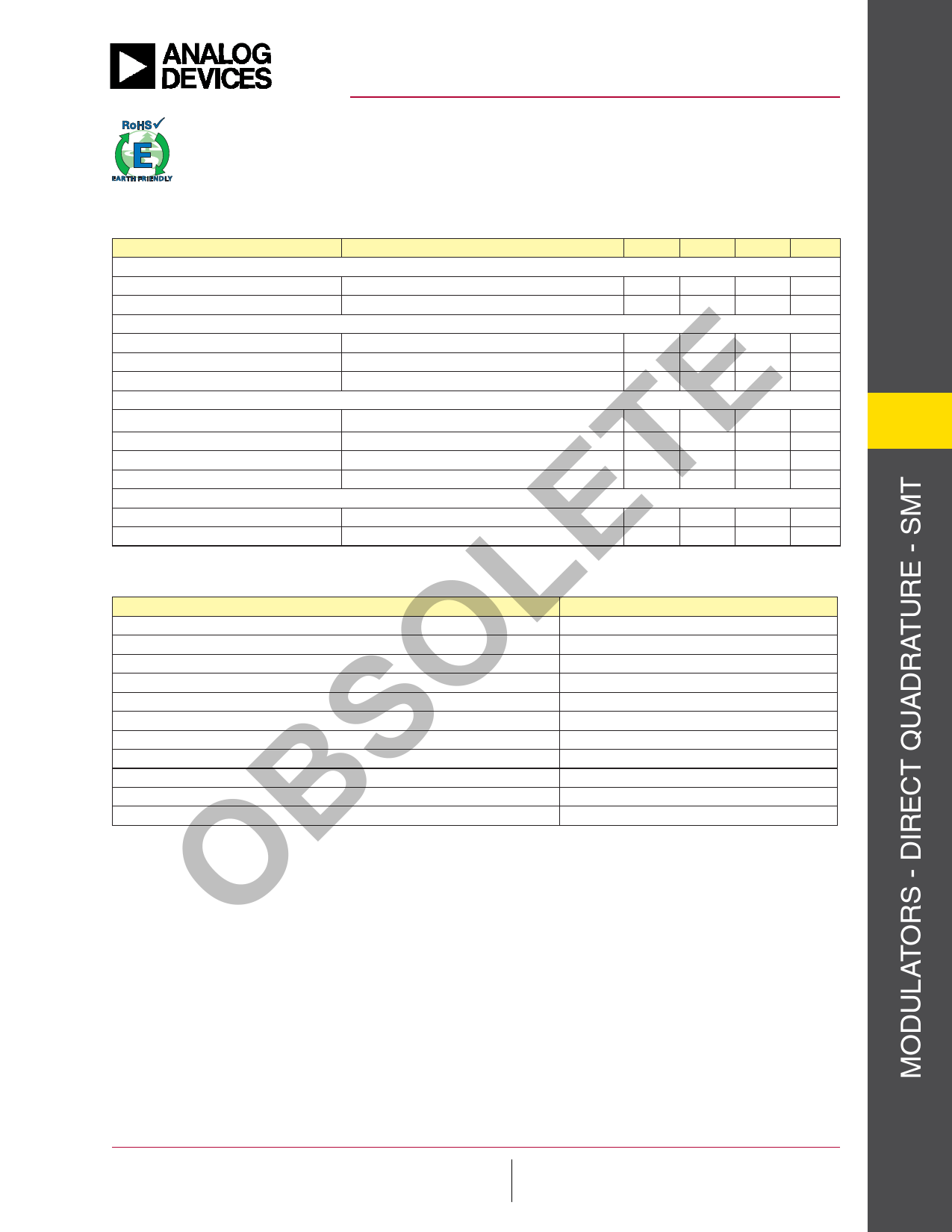
Electrical Specifications, (continued)
Parameter
Conditions
Min.
Typ.
Max. Units
RF Output
RF Frequency Range
100
4000
MHz
RF Return Loss
15
dB
LO Input
LO Frequency Range
LO Input Power
LO Port Return Loss
Baseband Input Port
Baseband Port Bandwidth
E Baseband Input DC Voltage (Vbbdc)
Baseband Input DC Bias Current (Ibbdc)
Single-ended Baseband Input Capacitance
T DC Power Requirements
Supply Voltage (Vcc1, Vcc2)
Supply Current (Icc1, Icc2)
3 dB Bandwidth with 50Ω source.
Single-ended.
De-embed to the lead of the device.
See Test Conditions Below
100
4000
MHz
-6
0
+6
dBm
15
dB
DC
700
MHz
+1.4
+1.5
+1.6
V
90
μA
4.5
pF
+4.5
+5.0
+5.5
V
168
mA
E Test Conditions: Unless Otherwise Specified, the Following Test Conditions Were Used
Parameter
L Temperature
Baseband Input Frequency
Baseband Input DC Voltage (Vbbdc)
Baseband Input AC Voltage
(Peak to Peak Differential, I and Q)
O Baseband Input AC Voltage for OIP3 Measurement (Peak to Peak Differential, I and Q)
Frequency Offset for Output Noise Measurements
Supply (Vcc1, Vcc2)
LO Input Power
S LO Input Mode
Mounting Configuration
Sideband & Carrier Feedthrough
Condition
+25 °C
200 kHz
+1.5V
1.6V
800 mV per tone @ 150 & 250 kHz
20 MHz
+5.0V
0 dBm
Single-Ended through LON
Refer to HMC497LP4 Application Schematic Herein
Uncalibrated
B Calibrated vs. Uncalibrated Test Results
During the Uncalibrated Sideband and Carrier Suppression tests, care is taken to ensure that the I/Q signal paths from
O the Vector Signal Generator (VSG) to the Device Under Test (DUT) are equal. The “Uncalibrated, +25 °C” Sideband
and Carrier Suppression plots were measured at room temperature, while the “Uncalibrated, over Temperature”
Sideband and Carrier Suppression plots represent the worst case uncalibrated suppression levels measured at T=
-40 °C, +25 °C, and +85 °C.
The “Calibrated, + 25 °C” Sideband Suppression data was plotted after a manual adjustment of the I/Q amplitude
balance and I/Q phase offset (skew) at +25 °C, and at each LO input power level. The +25 °C adjustment settings
were held constant during tests over temperature. The “Calibrated, over Temperature” plots represent the worst case
calibrated Sideband Suppression levels at T= -40 °C, +25 °C, and +85 °C.
The “Calibrated, +25 °C” Carrier Suppression data was plotted after a manual adjustment of the Ip/In & Qp/Qn DC
offsets at +25 °C, and at each LO input power level. The +25 °C adjustment settings were held constant during tests
over temperature. The “Calibrated, over Temperature” plots represent the worst case Carrier Suppression levels
measured at T= -40 °C, +25 °C, and +85 °C.
IrrliniecgfseohpntrsomsenoasftiisibtohingilrirtdyafunpirstnaeairdstsihesbesuydFmthimebao2dtyprmlb0iAcyapanyAtaAriorlnioenlacgspluooelDrhgt,eofDarvtodheimcevReericwistlesoiissivuseafseobeudr.rnei,dtSlyiseep,Cvureesacahdeinf,niyectnoadopltrmiabofttenoeossrnatasfcnopuocyrbulrjipaerndaacfcrttt,eientenogMatecnromhdiAgaerhnrndtegs0tlseieao1obwfrf8lAisepthn.2a,oatH4uelpotongwntlPseoDeotviheacreveoorsi,.ctheeNnnesoore. c:o9FOPnoh7ntroea8npcT-er2eti:cc57Heh80,n1it-od-t33leiot2l3gie9vy4e-M4rW3y7,ai0cyaF0,rna•Pod.xwOOt:or.ad9Bvep7orelax8ocCn9-e2l1ion0o5er6r0dp,aeN-otr3wosr3:raww7Atwoin3oo.aandlno,:agMloADge.0cv2oic0me6s2,-9In10c.6,
Trademarks and registered trademarks are the property of their resOpecrtdiveeorwnOerns. -line at www.hAipttpiltieca.ctioonmSupport: Phone: 1-800-ANALOG-D
10
10 - 25
Share Link: 