MSM9405MB データシートの表示(PDF) - Oki Electric Industry
部品番号
コンポーネント説明
一致するリスト
MSM9405MB Datasheet PDF : 30 Pages
| |||
¡ Semiconductor
MSM9405
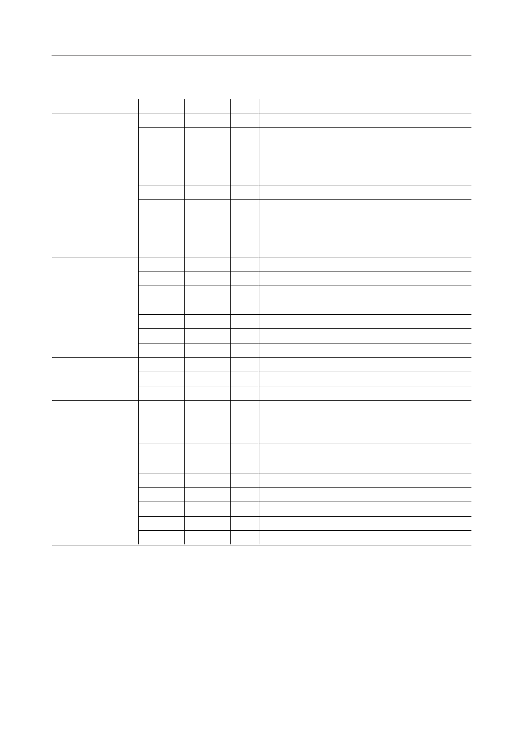
PIN DESCRIPTIONS
Function
Transceiver
Module Interface
Microcontroller
Interface
DMA Controller
Interface
Others
Pin
27
26
25
24
9-2
13-10
14
15
17
18
22
21
23
20
19
28
30
29
1
16
Symbol
IRIN-A
IRIN-B
IROUT
SD
D0-D7
A0-A3
CS
RD
WR
INTR
DREQ
DACK
TC
PWDN
RESET
TEST
XIN
XOUT
VDD
GND
Type
Description
I Receive signal input A. (2.4 kbps to 4 Mbps)*1
I Receive signal input B. (0.576 to 4 Mbps)
When connecting this device to a transceiver module,
tie this pin high or low if the number of the receive signal
output pins that the module has is only one.*1
O Transmit signal output. Active high.
O Transceiver module control signal output.
Becomes active when PWDN is set low.*1
This pin must be left open if connecting this device to a
transceiver module having no shutdown pins.
I/O Data input-output.
I Register address inputs.
I Chip select input. Active low.
When low, read and write signals are enabled.
I Read signal input. Active low.
I Write signal input. Active low.
O Interrupt request signal output. Active low.
O DMA Request signal output. *1
I DMA acknowledge signal input. *1
I DMA transfer end signal input. Active low.
I Power down control. Active low.
When set low, oscillation stops and the device enters power
down (low supply current) mode.
I System reset input. Active low.
When set low, the internal registers are initialized.
O Test. Must be left open.
I Crystal connect.
O Crystal connect.
— Power supply.
— Ground.
*1 Either active high or active low can be selected depending on the register setting.
4/30
Share Link: 