NTE932 データシートの表示(PDF) - NTE Electronics
部品番号
コンポーネント説明
一致するリスト
NTE932 Datasheet PDF : 2 Pages
| |||
Electrical Characteristics: (TJ = 0° to +125°C unless otherwise specified)
Parameter
Output Voltage
Input–Output Voltage
Differential
Line Regulation
Load Regulation
Quiescent Current
Quiescent Current, Line
Quiescent Current, Load
Current Limit
Temperature Coefficient
Output Noise Voltage
Ripple Attenuation
Power Dissipation
Symbol
Test Conditions
Min Typ Max Unit
VO TJ = +25°C, VIN = 8V to 15V, IO = 10mA to 5A, 4.75 5.00 5.25 V
Note 2
VIN–VO IO = 5A
2.6 –
–
V
Regline TJ = +25°C, VIN = 8V to 20V, IO = 3A, Note 3
–
– 1.0 %/VO
Regload TJ = +25°C, VIN = 8V, IO = 10mA to 5A, Note 3 –
– 0.6 %/VO
IQ TJ = +25°C, VIN = 8V, IO = 10mA
–
– 25 mA
IQ(Line) TJ = +25°C, VIN = 8V to 15V, IO = 10mA
–
–
5 mA
IQ(Load) TJ = +25°C, VIN = 8V, IO = 10mA to 5A
–
–
5 mA
ILIM TJ = +25°C, VIN = 10V, Note 2
–
– 15
A
TC VIN = 8V, IO = 100mA
–
–
5 mA
Vn VIN = 8V, IO = 100mA, f = 10Hz to 100kHz
–
–
10 µVrms
RA VIN = 10V, IO = 2A
60 –
–
dB
PD 2.6V to 10V (VIN – VO), IO = 10mA to 5A
–
– 50 W
Note 2. Low duty cycle pulse testing with Kelvin connections required. Die temperature changes
must be accounted for separately.
Note 3. Ripple attenuation is specified for a 1Vrms, 120Hz, input ripple. Ripple attenuation is
minimum of 60dB at 5V output and is 1dB less for each volt increase in the output volt-
age.
Note 4. VO = VC (1 + R1/R2) where:
R1 = Resistance from output to control
R2 = Resistance from control to common
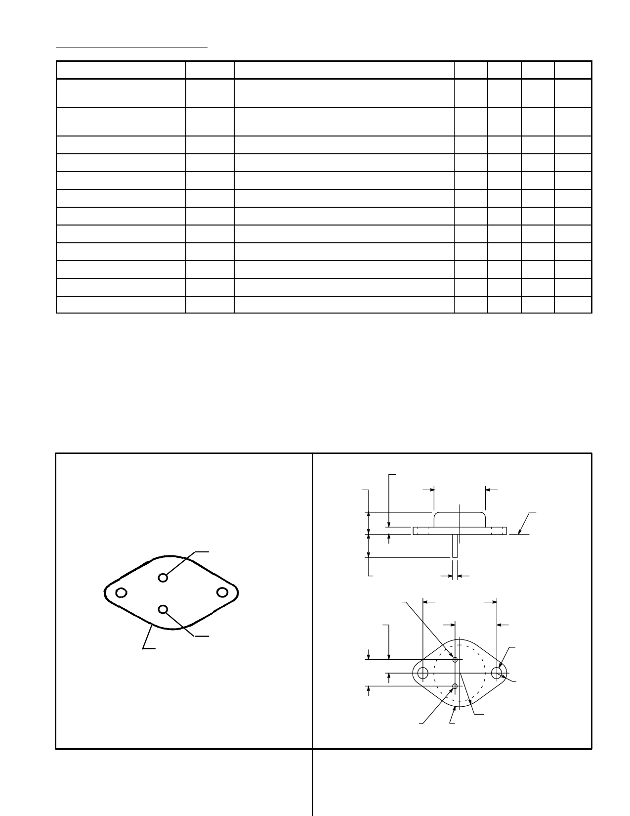
Pin Connection Diagram
Output
2
1
Input
Case/GND
.350 (8.89)
.135 (3.45) Max
.875 (22.2)
Dia Max
Seating
Plane
.312 (7.93) Min
.040 (1.02)
VOUT
.215 (5.45)
.430
(10.92)
1.187 (30.16)
.665
(16.9)
.156 (3.96) Dia
(2 Holes)
.188 (4.8) R Max
.525 (13.35) R Max
VIN
GND/Case
Share Link: 