ICS670-01 データシートの表示(PDF) - Integrated Circuit Systems
部品番号
コンポーネント説明
一致するリスト
ICS670-01 Datasheet PDF : 5 Pages
| |||
ICS670-01
Low Phase Noise Zero Delay Buffer and Multiplier
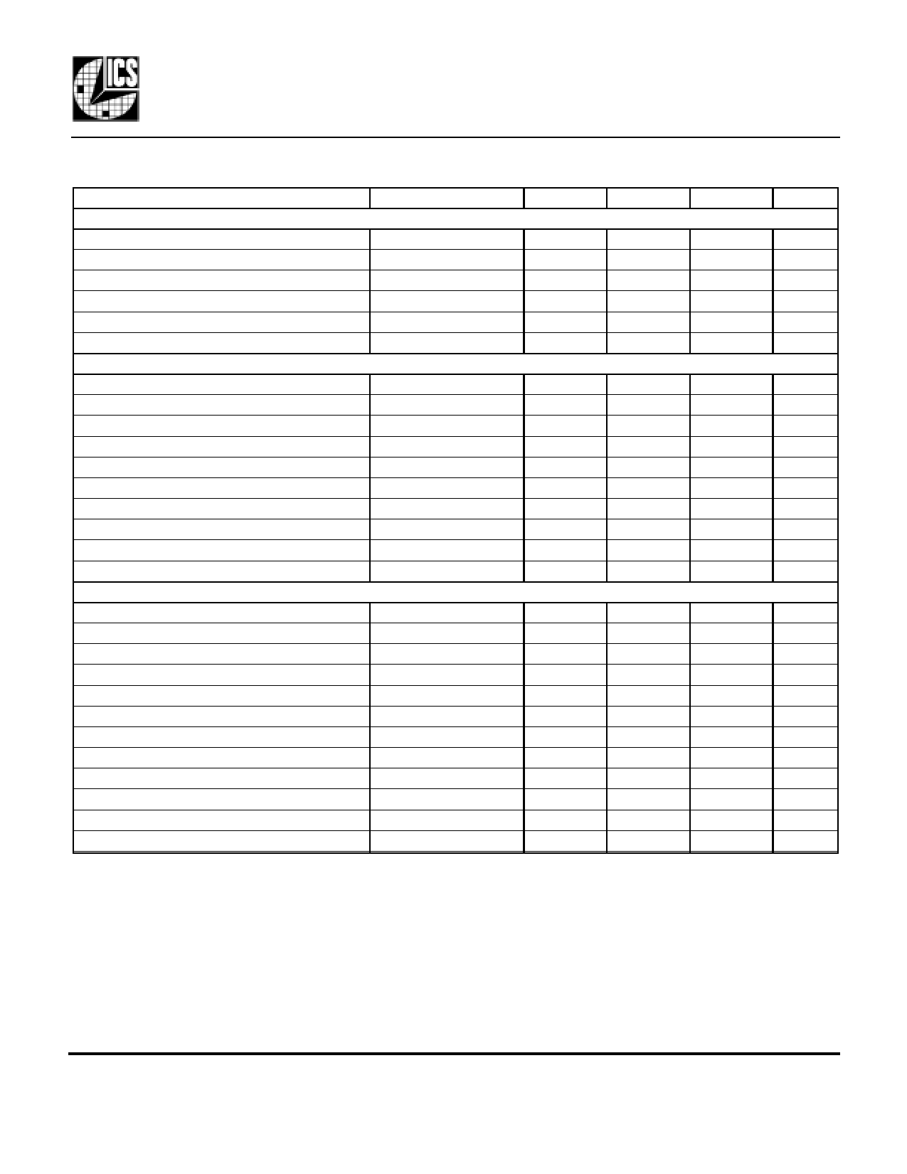
Electrical Specifications
Parameter
Conditions
ABSOLUTE MAXIMUM RATINGS (note 1)
Supply voltage, VDD
Referenced to GND
Inputs and Clock Outputs
Referenced to GND
Ambient Operating Temperature
Ambient Operating Temperature, ICS670M-01I Industrial temperature
Soldering Temperature
Max of 10 seconds
Storage temperature
DC CHARACTERISTICS (VDD = 3.3 V unless noted)
Operating Voltage, VDD
Input High Voltage, VIH
Input Low Voltage, VIL
Output High Voltage, VOH, CMOS level
IOH=-4mA
Output High Voltage, VOH
IOH=-12mA
Output Low Voltage, VOL
IOL=12mA
Operating Supply Current, IDD
No Load
Short Circuit Current
Each output
Internal Pull-up Resistor
OE, select pins
Input Capacitance
OE, select pins
AC CHARACTERISTICS (VDD = 3.3 V unless noted)
Input Frequency (see table on page 2)
Depends on multiplier
Output Frequency
at 3.3V or 5V
Output Clock Rise Time
0.8 to 2.0V, no load
Output Clock Fall Time
0.8 to 2.0V, no load
Output Clock Duty Cycle
At VDD/2
Input to output skew, rising edges
Note 2
Maximum Absolute Jitter, short term
Maximum Jitter, one sigma
Phase Noise, relative to carrier, 125 MHz (x5) 100 Hz offset
Phase Noise, relative to carrier, 125 MHz (x5) 1 kHz offset
Phase Noise, relative to carrier, 125 MHz (x5) 10 kHz offset
Phase Noise, relative to carrier, 125 MHz (x5) 100 kHz offset
Minimum
-0.5
0
-40
-65
3.0
2
VDD-0.4
2.4
5
45
Typical
35
±50
200
5
50
±100
±45
15
-110
-122
-121
-117
Maximum Units
7
V
VDD+0.5
V
70
°C
85
°C
260
°C
150
°C
5.5
V
V
0.8
V
V
V
0.4
V
mA
mA
kΩ
pF
160
MHz
160
MHz
1.5
ns
1.5
ns
55
%
ps
ps
ps
dBc/Hz
dBc/Hz
dBc/Hz
dBc/Hz
Notes:
1. Stresses beyond those listed under Absolute Maximum Ratings could cause permanent damage to the device. Prolonged
exposure to levels above the operating limits but below the Absolute Maximums may affect device reliability.
2. Rising edge of ICLK compared with rising edge of CLK2, with FBCLK connected to FBIN, and 15 pF load on CLK2.
See the graph on page 4 for skew versus frequency and loading.
MDS 670-01 B
3
Revision 100900
Printed 11/15/00
Integrated Circuit Systems • 525 Race Street • San Jose •CA•95126•(408) 295-9800tel•http://www.icst.com
Share Link: 