HIP1011A データシートの表示(PDF) - Renesas Electronics
部品番号
コンポーネント説明
一致するリスト
HIP1011A Datasheet PDF : 12 Pages
| |||
HIP1011A
Absolute Maximum Ratings
VCC, 12VIN . . . . . . . . . . . . . . . . . . . . . . . . . . . . . . . -0.5V to +14.0V
12VO . . . . . . . . . . . . . . . . . . . . . . . . . . . . . . . -0.5V to V12VIN +0.5V
12VO, 12VG, 3V5VG . . . . . . . . . . . . . . . . . . . . . -0.5V to VCC +0.5V
M12VIN . . . . . . . . . . . . . . . . . . . . . . . . . . . . . . . . . . -15.0V to +0.5V
M12VO, M12VG. . . . . . . . . . . . . . . . . . . . . . VM12VIN-0.5V to +0.5V
3VISEN, 5VISEN . . . . . . . . . . . -0.5V to the Lesser of VCC or +7.0V
Voltage, Any Other Pin . . . . . . . . . . . . . . . . . . . . . . . -0.5V to +7.0V
12VO Output Current . . . . . . . . . . . . . . . . . . . . . . . . . . . . . . . . . . .3A
M12VO Output Current . . . . . . . . . . . . . . . . . . . . . . . . . . . . . . . 0.8A
ESD Classification . . . . . . . . . . . . . . . . . . . . . . . . . . . . . 4KeV (HBM)
Thermal Information
Thermal Resistance (Typical, Note 1)
JA (oC/W)
SOIC Package . . . . . . . . . . . . . . . . . . . . . . . . . . . . .
105
Maximum Junction Temperature . . . . . . . . . . . . . . . . . . . . . .125oC
Maximum Storage Temperature Range . . . . . . . . . -65oC to 150oC
Maximum Lead Temperature (Soldering 10s) . . . . . . . . . . . . .300oC
(SOIC - Lead Tips Only)
Die Characteristics
Number of Transistors . . . . . . . . . . . . . . . . . . . . . . . . . . . . . . . . . 290
Operating Conditions
VCC Supply Voltage Range. . . . . . . . . . . . . . . . . . +10.8V to +13.2V
12V, 5V and 3.3V Input Supply Tolerances 10%
12VO Output Current . . . . . . . . . . . . . . . . . . . . . . . . . . . . .0 to +0.5A
M12VO Output Current . . . . . . . . . . . . . . . . . . . . . . . . . . .0 to +0.1A
Temperature Range (TA) . . . . . . . . . . . . . . . . . . . . . . . . 0oC to 70oC
CAUTION: Stresses above those listed in “Absolute Maximum Ratings” may cause permanent damage to the device. This is a stress only rating and operation of the
device at these or any other conditions above those indicated in the operational sections of this specification is not implied.
NOTES:
1. JA is measured with the component mounted on a low effective thermal conductivity test board in free air. See Tech Brief 379 for details.
2. All voltages are relative to GND, unless otherwise specified.
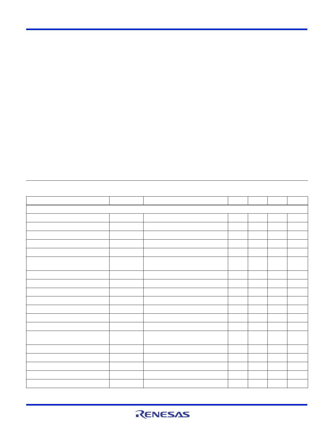
Electrical Specifications
PARAMETER
5V/3.3V SUPPLY CONTROL
Nominal 5.0V and 3.3V Input Supply Voltages,
VCC = 12VIN = 12V, M12VIN = -12V, TA = TJ = 0 to 70oC, Unless Otherwise Specified
SYMBOL
TEST CONDITIONS
MIN
TYP
5V Overcurrent Threshold
5V Overcurrent Threshold Voltage
5V Overcurrent Threshold Voltage
5V Undervoltage Trip Threshold
5V Undervoltage Fault Response Time
5V Turn-On Time
(PWRON High to 5VOUT = 4.75V)
5VS Input Bias Current
5VISEN Input Bias Current
3V Overcurrent Threshold
3V Overcurrent Threshold Voltage
3V Overcurrent Threshold Voltage
3V Undervoltage Trip Threshold
3V Undervoltage Fault Response Time
3V Turn-On Time
(PWRON High to 3VOUT = 3.00V)
3VS Input Bias Current
3VISEN Input Bias Current
3V5VG Vout Low
IOC5V
See Typical Application Diagram
VOC5V_1 VOCSET = 0.6V
VOC5V_2 VOCSET = 1.2V
V5VUV
t5VUV
tON5V
C3V5VG = 0.022F, C5VOUT = 2000F,
RL = 1
IB5VS
PWRON = High
IB5VISEN PWRON = High
IOC3V
See Typical Application Diagram
VOC3V_1 VOCSET = 0.6V
VOC3V_2 VOCSET = 1.2V
V3VUV
t3VUV
tON3V
C3V5VG = 0.022F, C3VOUT = 2000F,
RL = 0.43
IB3VS
PWRON = High
IB3VISEN PWRON = High
Vout_lo_35VG PWRON = Low, FLTN = Low
-
30
66
4.42
-
-
-40
-160
-
42
88
2.74
-
-
-40
-160
-
7.1
36
72
4.65
150
6.5
-26
-140
9.0
49
95
2.86
150
6.5
-26
-140
0.1
3V5VG Vout High
Vout_hi_35VG PWRON = High, FLTN = High
10.5
11.1
Gate Output Charge Current
IC3V5VG PWRON = High, V3V5VG = 2V
22.5
25.0
MAX UNITS
-
A
42
mV
79
mV
4.75
V
350
ns
-
ms
-20
A
-110
A
-
A
56
mV
102
mV
2.97
V
350
ns
-
ms
-20
A
-110
A
0.4
V
-
V
27.5
A
FN4631 Rev 5.00
November 16, 2004
Page 4 of 11
Share Link: 