P4C116 データシートの表示(PDF) - Semiconductor Corporation
部品番号
コンポーネント説明
一致するリスト
P4C116 Datasheet PDF : 14 Pages
| |||
P4C116/P4C116L
AC CHARACTERISTICS—WRITE CYCLE
(VCC = 5V ± 10%, All Temperature Ranges)(2)
Sym.
Parameter
–10
–12
–15
–20
–25
–35
Min Max Min Max Min Max Min Max Min Max Min Max
tWC Write Cycle Time
10
12
15
20
25
35
tCW Chip Enable Time to End of Write 8
tAW Address Valid to End of Write
8
tAS Address Set-up Time
0
tWP Write Pulse Width
8
tAH Address Hold Time
0
tDW Data Valid to End of Write
7
tDH Data Hold Time
0
tWZ Write Enable to Output in High Z
tOW Output Active from End of Write 0
10
12
15
18
25
10
12
15
18
25
0
0
0
0
0
10
12
15
18
20
0
0
0
0
0
8
10
12
15
20
0
0
0
0
0
6
7
8
10
15
15
0
0
0
0
0
Unit
ns
ns
ns
ns
ns
ns
ns
ns
ns
ns
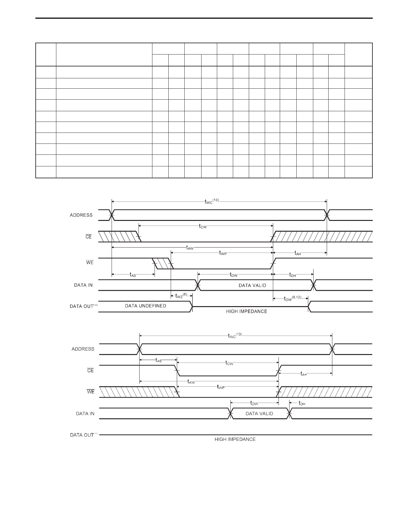
TIMING WAVEFORM OF WRITE CYCLE NO. 1 (WE CONTROLLED)(10,11)
TIMING WAVEFORM OF WRITE CYCLE NO. 2 (CE CONTROLLED)(10)
Notes:
10. CE and WE must be LOW for WRITE cycle.
11. OE is LOW for this WRITE cycle to show tWZ and tOW.
12. If CE goes HIGH simultaneously with WE HIGH, the output remains
in a high impedance state
13. Write Cycle Time is measured from the last valid address to the first
transitioning address.
Document # SRAM110 REV A
Page 5 of 14
Share Link: 