MC74HCT541 データシートの表示(PDF) - Motorola => Freescale
部品番号
コンポーネント説明
一致するリスト
MC74HCT541
Motorola => Freescale

MC74HCT541 Datasheet PDF : 5 Pages
| |||
MC74HCT541A
PIN DESCRIPTIONS
INPUTS
A1, A2, A3, A4, A5, A6, A7, A8 (PINS 2, 3, 4, 5, 6, 7, 8,
9) — Data input pins. Data on these pins appear in non–in-
verted form on the corresponding Y outputs, when the out-
puts are enabled.
CONTROLS
OE1, OE2 (PINS 1, 19) — Output enables (active–low).
When a low voltage is applied to both of these pins, the out-
puts are enabled and the device functions as a non–inverting
buffer. When a high voltage is applied to either input, the out-
puts assume the high impedance state.
OUTPUTS
Y1, Y2, Y3, Y4, Y5, Y6, Y7, Y8 (PINS 18, 17, 16, 15, 14,
13, 12, 11) — Device outputs. Depending upon the state of
the output enable pins, these outputs are either non–invert-
ing outputs or high–impedance outputs.
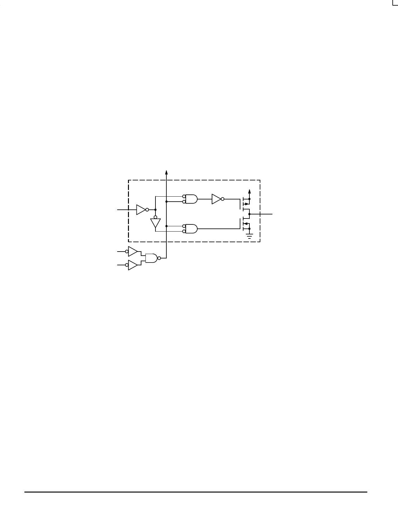
LOGIC DETAIL
To 7 Other
Buffers
INPUT A
One of Eight
Buffers
VCC
OUTPUT Y
OE1
OE2
MOTOROLA
3–4
High–Speed CMOS Logic Data
DL129 — Rev 6
Share Link: