W194 データシートの表示(PDF) - Cypress Semiconductor
部品番号
コンポーネント説明
一致するリスト
W194 Datasheet PDF : 6 Pages
| |||
W194
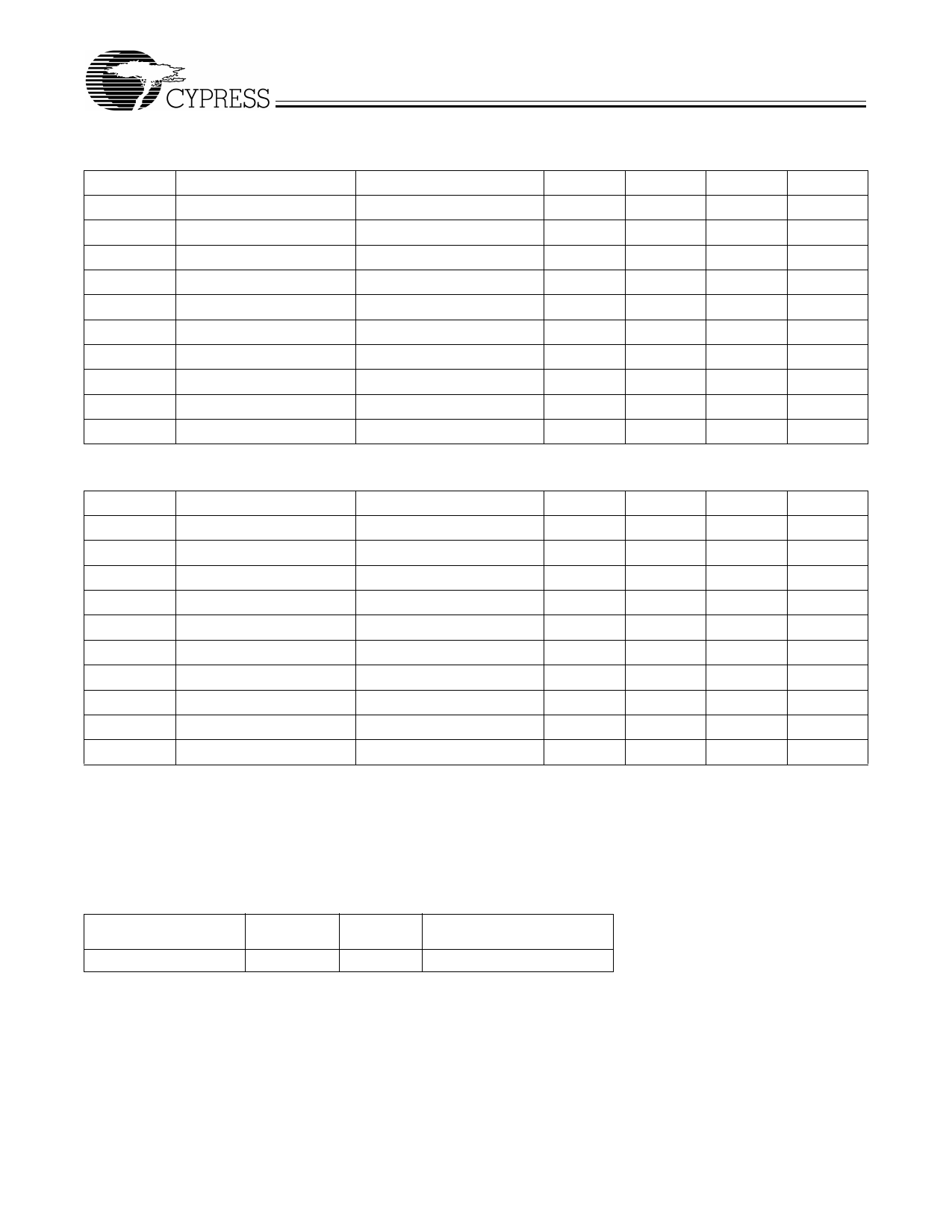
AC Electrical Characteristics: TA = 0°C to +70°C, VDD = 3.3V ±5%
Parameter
Description
Test Condition
Min
Typ
Max
Unit
fIN
Input Frequency[1]
OUT2 = REF
fOUT
Output Frequency
OUT1 15-pF load[6]
10
MHz
133
MHz
tR
Output Rise Time
2.0V to 0.8V, 15-pF load
3.5
ns
tF
Output Fall Time
2.0V to 0.8V, 15-pF load
2.5
ns
tICLKR
Input Clock Rise Time[2]
10
ns
tICLKF
Input Clock Fall Time[2]
10
ns
tPD
FBIN to REF Skew[3, 4]
Measured at VDD/2
–2
0.6
2
ns
tD
Duty Cycle
15-pF load[5]
40
50
60
%
tLOCK
PLL Lock Time
Power supply stable
1.0
ms
tJC
Jitter, Cycle-to-Cycle
300
ps
AC Electrical Characteristics: TA = 0°C to +70°C, VDD = 5.0V ±10%
Parameter
Description
Test Condition
Min
Typ
Max
Unit
fIN
Input Frequency[1]
OUT2 = REF
fOUT
Output Frequency
OUT1 15-pF load[6]
10
MHz
133
MHz
tR
Output Rise Time
2.0V to 0.8V, 15-pF load
2.5
ns
tF
Output Fall Time
2.0V to 0.8V, 15-pF load
1.5
ns
tICLKR
Input Clock Rise Time[2]
10
ns
tICLKF
Input Clock Fall Time[2]
10
ns
tPD
FBIN to REF Skew[3, 4]
Measured at VDD/2
–2
0.6
2
ns
tD
Duty Cycle
15-pF load[5, 7]
40
50
60
%
tLOCK
PLL Lock Time
Power supply stable
1.0
ms
tJC
Jitter, Cycle-to-Cycle
200
ps
Notes:
1. Input frequency is limited by output frequency range and input to output frequency multiplication factor (which is determined by circuit configuration).
2. Longer input rise and fall time will degrade skew and jitter performance.
3. All AC specifications are measured with a 50Ω transmission line, load terminated with 50Ω to 1.4V.
4. Skew is measured at 1.4V on rising edges.
5. Duty cycle is measured at 1.4V.
6. For the higher drive -11, the load is 20 pF.
7. Duty Cycle measured at 120 MHz. For 133 MHz, degrades to 35/65 worst case.
Ordering Information
Ordering Code
W194
Document #: 38-00794-A
Option
-70
Package
Name
G
Package Type
8-pin SOIC (150-mil)
5
Share Link: 