FW156 データシートの表示(PDF) - SANYO -> Panasonic
部品番号
コンポーネント説明
一致するリスト
FW156 Datasheet PDF : 4 Pages
| |||
Continued from preceding page.
Parameter
Turn-ON Delay Time
Rise Time
Turn-OFF Delay Time
Fall Time
Total Gate Charge
Gate-to-Source Charge
Gate-to-Drain “Miller” Charge
Diode Forward Voltage
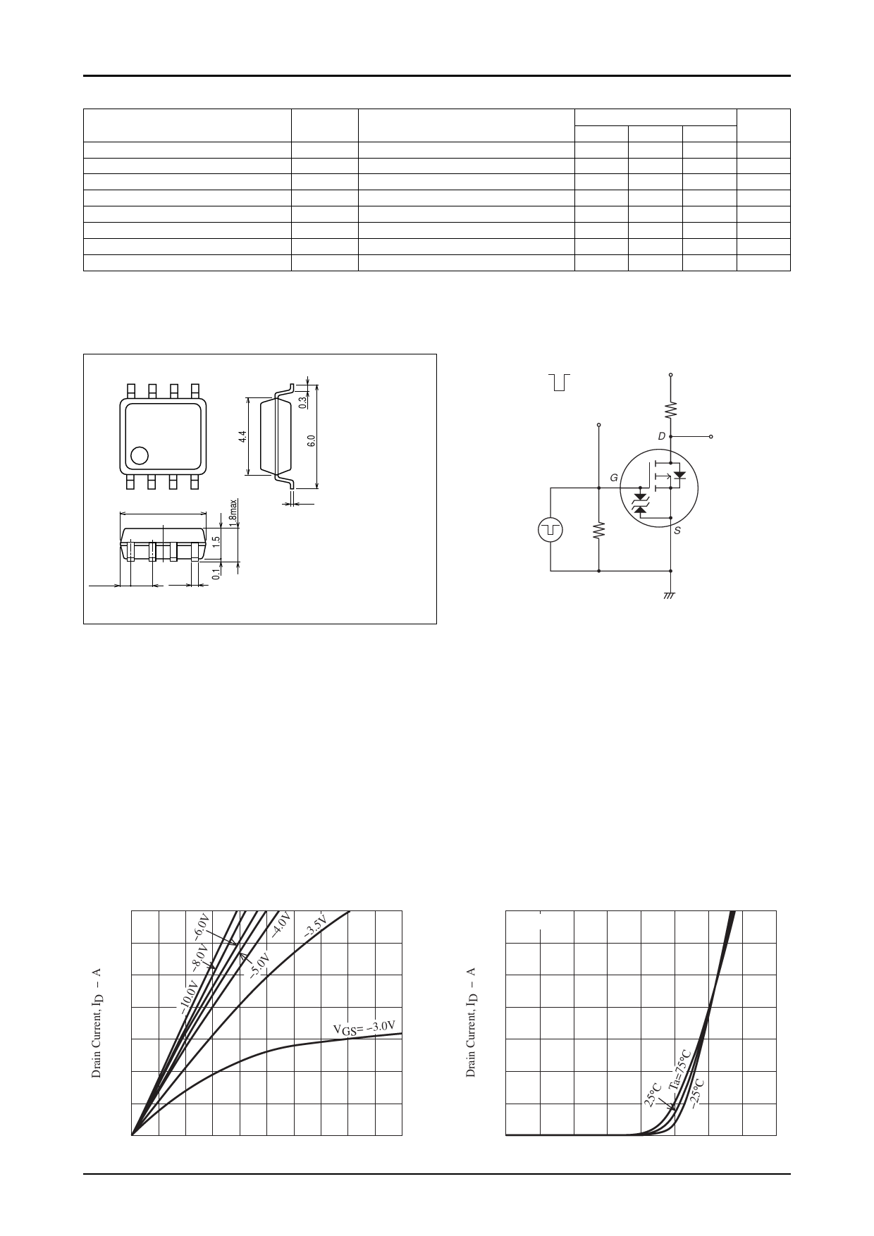
Package Dimensions
unit : mm
2129
8
5
1
4
5.0
0.595 1.27 0.43
FW156
Symbol
td(on)
tr
td(off)
tf
Qg
Qgs
Qgd
VSD
Conditions
See specified Test Circuit.
See specified Test Circuit.
See specified Test Circuit.
See specified Test Circuit.
VDS=--30V, VGS=--10V, ID=--3.5A
VDS=--30V, VGS=--10V, ID=--3.5A
VDS=--30V, VGS=--10V, ID=--3.5A
IS=--3.5A, VGS=0
Ratings
Unit
min
typ
max
12
ns
50
ns
100
ns
65
ns
22
nC
4
nC
4
nC
--0.86
--1.2
V
Switching Time Test Circuit
1 : Source1
2 : Gate1
3 : Source2
0.2 4 : Gate2
5 : Drain2
6 : Drain2
7 : Drain1
8 : Drain1
SANYO : SOP8
VIN
0V
--10V
VIN
PW=10µs
D.C.≤1%
G
VDD= --30V
ID= --2A
RL=15Ω
D
VOUT
FW156
P.G
50Ω
S
ID -- VDS
--3.5
--3.5V
--3.0
--2.5
--2.0
--1.5
VGS= --3.0V
--1.0
--0.5
0
0 --0.1 --0.2 --0.3 --0.4 --0.5 --0.6 --0.7 --0.8 --0.9 --1.0
Drain-to-Source Voltage, VDS -- V IT07094
--7
VDS= --10V
--6
ID -- VGS
--5
--4
--3
--2
--1
0
0 --0.5 --1.0 --1.5 --2.0 --2.5 --3.0 --3.5 --4.0
Gate-to-Source Voltage, VGS -- V IT07095
No.7784-2/4
Share Link: 