AS5C4008 データシートの表示(PDF) - Austin Semiconductor
部品番号
コンポーネント説明
一致するリスト
AS5C4008 Datasheet PDF : 17 Pages
| |||
Austin Semiconductor, Inc.
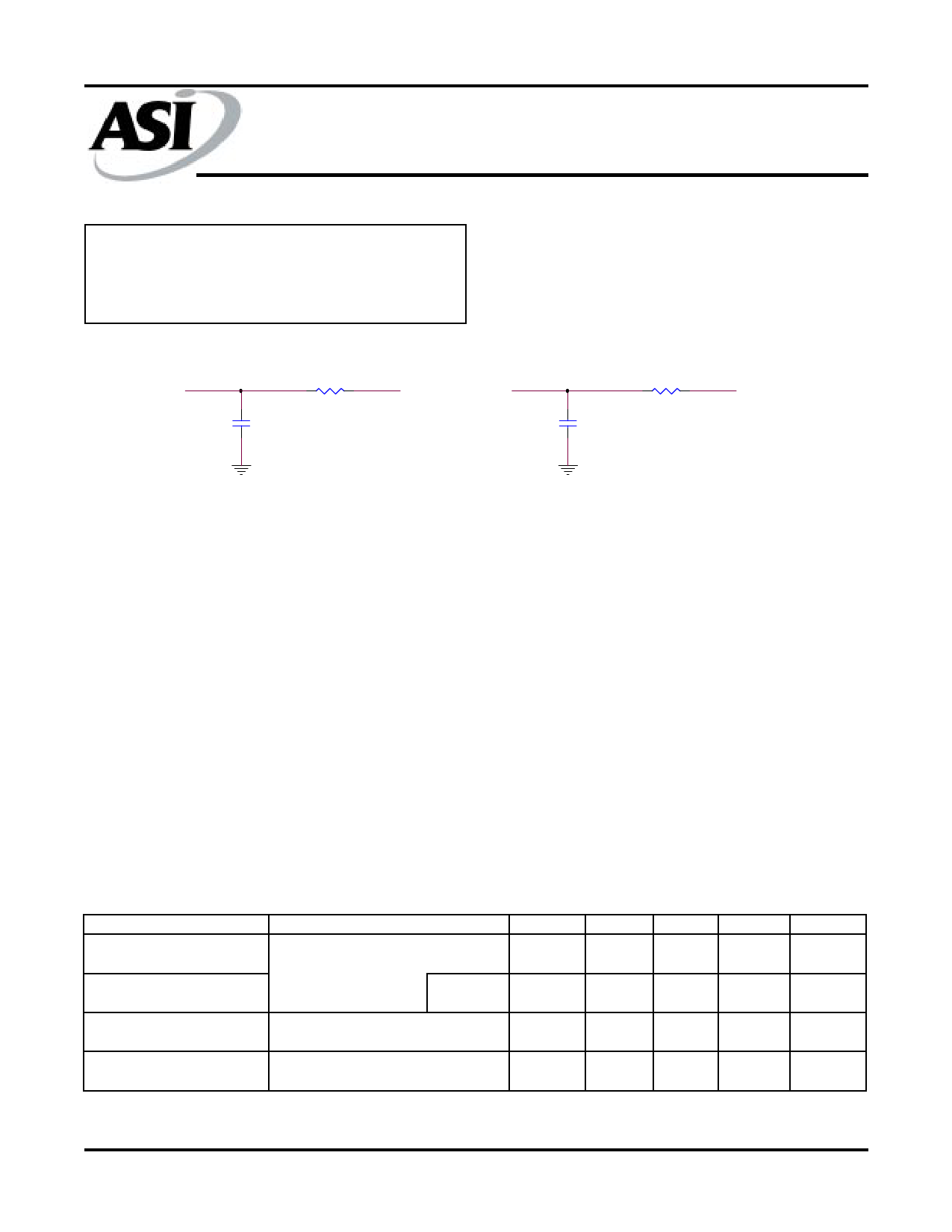
AC TEST CONDITIONS
Input pulse levels ................................................... Vss to 3.0V
Input rise and fall times ....................................................... 3ns
Input timing reference levels ............................................ 1.5V
Output reference levels ..................................................... 1.5V
Output load ............................................... See Figures 1 and 2
SRAM
AS5C4008
Q
167 ohms
1.73V
Q
167 ohms
1.73V
C=30pF
C=5pF
Fig. 1 Output Load Equivalent
Fig. 2 Output Load Equivalent
NOTES
1. All voltages referenced to VSS (GND).
2. -2V for pulse width < 20ns
3. I is dependent on output loading and cycle rates.
CC
4. This parameter is guaranteed but not tested.
5. Test conditions as specified with the output loading
as shown in Fig. 1 unless otherwise noted.
6. tLZCE, tLZWE, tLZOE, tHZCE, tHZOE and tHZWE
are specified with CL = 5pF as in Fig. 2. Transition is
measured ±200mV from steady state voltage.
7. At any given temperature and voltage condition,
tHZCE is less than tLZCE, and tHZWE is less than
tLZWE.
8. WE\ is HIGH for READ cycle.
9. Device is continuously selected. Chip enables and
output enables are held in their active state.
10. Address valid prior to, or coincident with, latest
occurring chip enable.
11. tRC = Read Cycle Time.
12. Chip enable and write enable can initiate and
terminate a WRITE cycle.
13. Output enable (OE\) is inactive (HIGH).
14. Output enable (OE\) is active (LOW).
15. ASI does not warrant functionality nor reliability of any
product in which the junction temperature exceeds
150°C. Care should be taken to limit power to acceptable
levels.
DATA RETENTION ELECTRICAL CHARACTERISTICS (L Version Only)
DESCRIPTION
VCC for Retention Data
Data Retention Current
(L Version Only)
Chip Deselect to Data
Retention Time
CONDITIONS
CE\ > (Vcc -0.2V)
VIN > (Vcc -0.2V) or < 0.2V
SYMBOL MIN
VDR
2
VCC = 2V ICCDR
tCDR
0
MAX
4.5
Operation Recovery Time
tR
10
UNITS
V
mA
ns
ms
NOTES
4
4, 11
AS5C4008
Rev. 5.5 12/01
Austin Semiconductor, Inc. reserves the right to change products or specifications without notice.
5
Share Link: 