AS5020 データシートの表示(PDF) - austriamicrosystems AG
部品番号
コンポーネント説明
一致するリスト
AS5020 Datasheet PDF : 11 Pages
| |||
6-Bit Magnetic Position Encoder –Data Sheet Rev.1.0
AS5020
Pin Description
Pin # Symbol Type Description
1
DATA DO DATA Output of the SSI.
If PD/CS=0, the measured angle data (6bit value) is serially
shifted out over this pin by the CLK, starting with the MSB. A
NVR Bit and a Parity bit are added. (NVR=1 indicates a Non-
Valid Range of the magnetic field.) Even Parity is given.
2
VDD
AI Positive Supply Voltage.
3
VSS
AI Negative Supply Voltage (GND).
4
PROG
DI PROGramming Input.
This pin is used to program the zero position into a non-volatile
memory (OTP). The programmed value is subtracted from the
actual measured angle.
5
N.C.
AI Not Connected during operation. This pin is used for testing
purposes.
6
N.C.
AI Not Connected during operation. This pin is used for testing
purposes.
7 PD/CS DI Power Down Input, Disable or Chip Select (active low).
PD/CS=0 activates the device and enables the measurement.
PD/CS=1 sets the device in power save mode and puts the
DATA pin in high impedance (highZ) state.
8
CLK
DI CLOCK Input of the SSI.
This pin is used to serially clock out the measured angle data at
Pin 7 (DATA).
DI: Digital Input
DO: Digital Output
MSB: Most Significant Bit
LSB: Least Significant Bit
Note: The pins 5 and 6 must not be connected!
AI:
Analogue Input
OTP: One Time Programmable
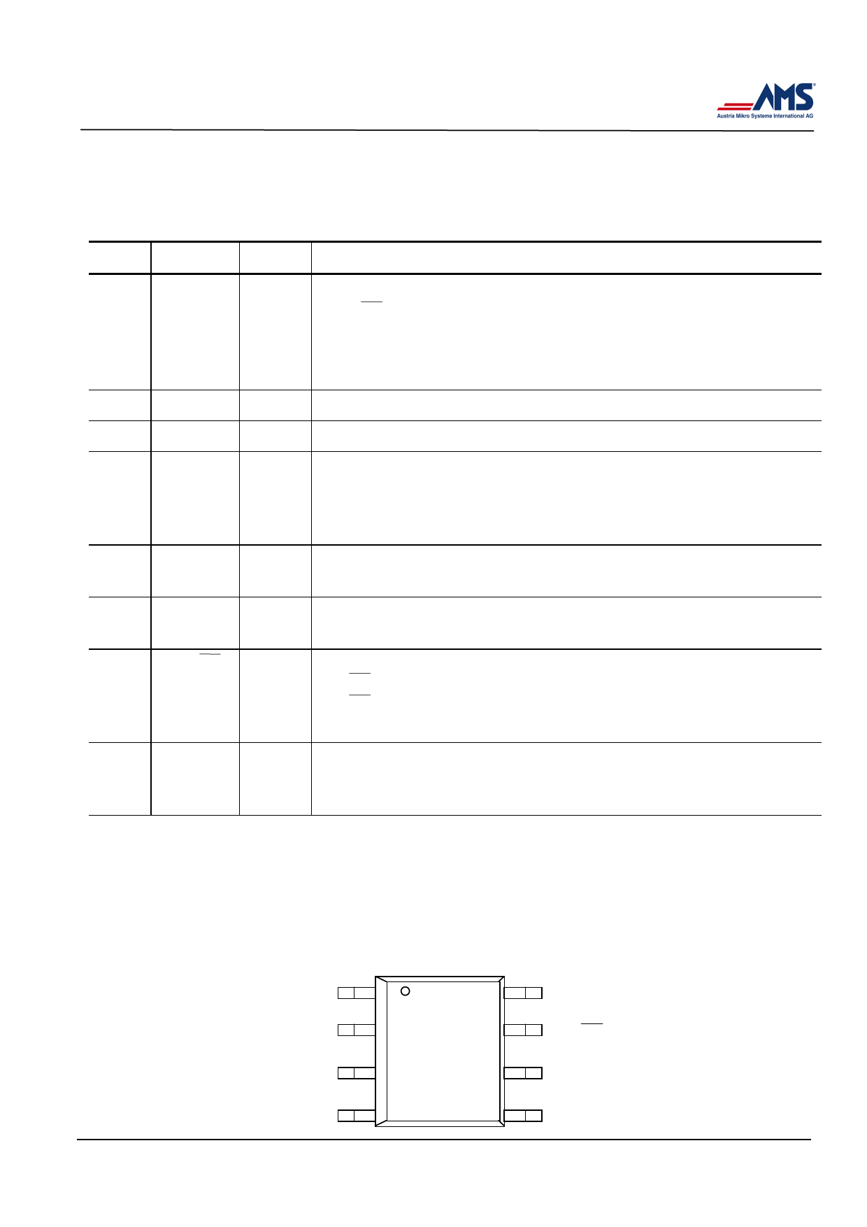
Pin Configuration
Rev. n/c
DATA
VDD
VSS
PROG
Page 2/11
CLK
PD/CS
N.C.
N.C.
Feb 2001
Share Link: 