TK75002DIMG データシートの表示(PDF) - Toko America Inc
部品番号
コンポーネント説明
一致するリスト
TK75002DIMG Datasheet PDF : 10 Pages
| |||
TK75002
APPLICATION INFORMATION
THE PARASITIC ZERO AND HOW IT IS ELIMINATED IN
THE TK75002
In a feedback-regulated isolated power supply, isolation is
usually provided by an opto-coupler whose photodiode
section is connected between the output of the power
supply and the output of the error amplifier (in series with
a resistor that converts the voltage difference between the
two outputs into a current). Due to the feed-forward path
established by that connection, the transfer function of the
error amplifier is significantly modified (the modification in
the transfer function appears also if the opto-coupler is
replaced by the combination of a transformer and peak
detector driven by a pulse amplitude modulator).
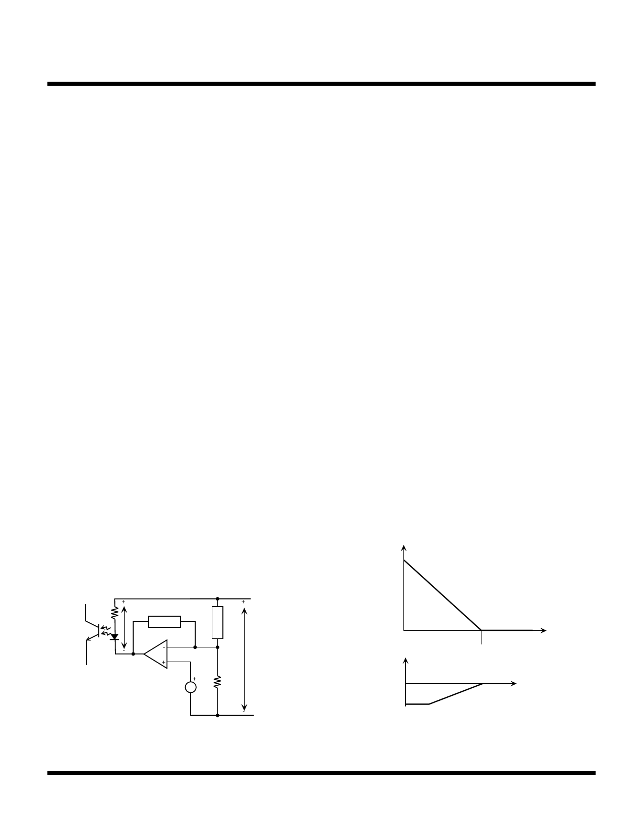
Figure 2 shows the error amplifier/opto-coupler
combination. The output voltage V2 (that is the voltage
measured across the photodiode and the series resistor)
can be written as:
V2 = V1 - [ - (ZFB / ZIN) x V1]
(1)
From (1), the transfer function of the error amplifier (from
the supply voltage V1, to the voltage V2) is:
H(s) = V2(s) / V1(s) = 1 + (ZFB / ZIN)
(2)
Figure 3 shows the magnitude and phase diagram of the
transfer function. As can be seen, the feed-forward path
adds a left half-plane zero (sometimes called a "parasitic"
zero) to the transfer function of the ideal integrator. The
parasitic zero is undesirable because it increases the high
frequency loop gain of the system, potentially leading to
subharmonic instability or chaotic behavior. To avoid the
effect of the zero, either a low pass (decoupling) filter must
be added to the supply rail of the opto-coupler, or an
additional pole must be introduced around the frequency
of the zero, or the loop gain must be reduced. (Note that
reducing the loop gain slows down the transient response
of the system.)
The TK75002 eliminates the parasitic zero by changing
the reference point of the error signal from the GND pin to
the VCC pin. That is achieved by inserting a level shifter
circuit between the output of the error amplifier and the
buffer of the pulse-amplitude modulator (see Figure 4).
The output voltage of the level shifter is proportional to the
error signal (i.e., the voltage of the COMP pin) and is
conveyed relative to the supply voltage V1. The end result
is that the transfer function becomes:
H(s) = ZFB / ZIN
(4)
In the case when the feedback impedance is a capacitor C
and the input impedance is a resistor R, the transfer
function becomes:
In the case of a capacitive feedback impedance and
resistive input impedance, the transfer function will be that
of an ideal integrator, without the parasitic zero.
H(s) = (1 + SRC) / SRC
H (dB)
(3)
-20 dB / dec
V2
ZFB
ZIN
V1
RB
Vref
FIGURE 2: ERROR AMPLIFIER / OPTO-COUPLER
COMBINATION
0
φ
0°
-90 °
f
1 / (2πRC)
f
FIGURE 3: MAGNITUDE AND PHASE VS.
FREQUENCY OF AN ERROR AMPLIFIER / OPTO-
COUPLER COMBINATION
Page 6
January 1999 TOKO, Inc.
Share Link: 