RF2363 データシートの表示(PDF) - RF Micro Devices
部品番号
コンポーネント説明
一致するリスト
RF2363 Datasheet PDF : 12 Pages
| |||
RF2363
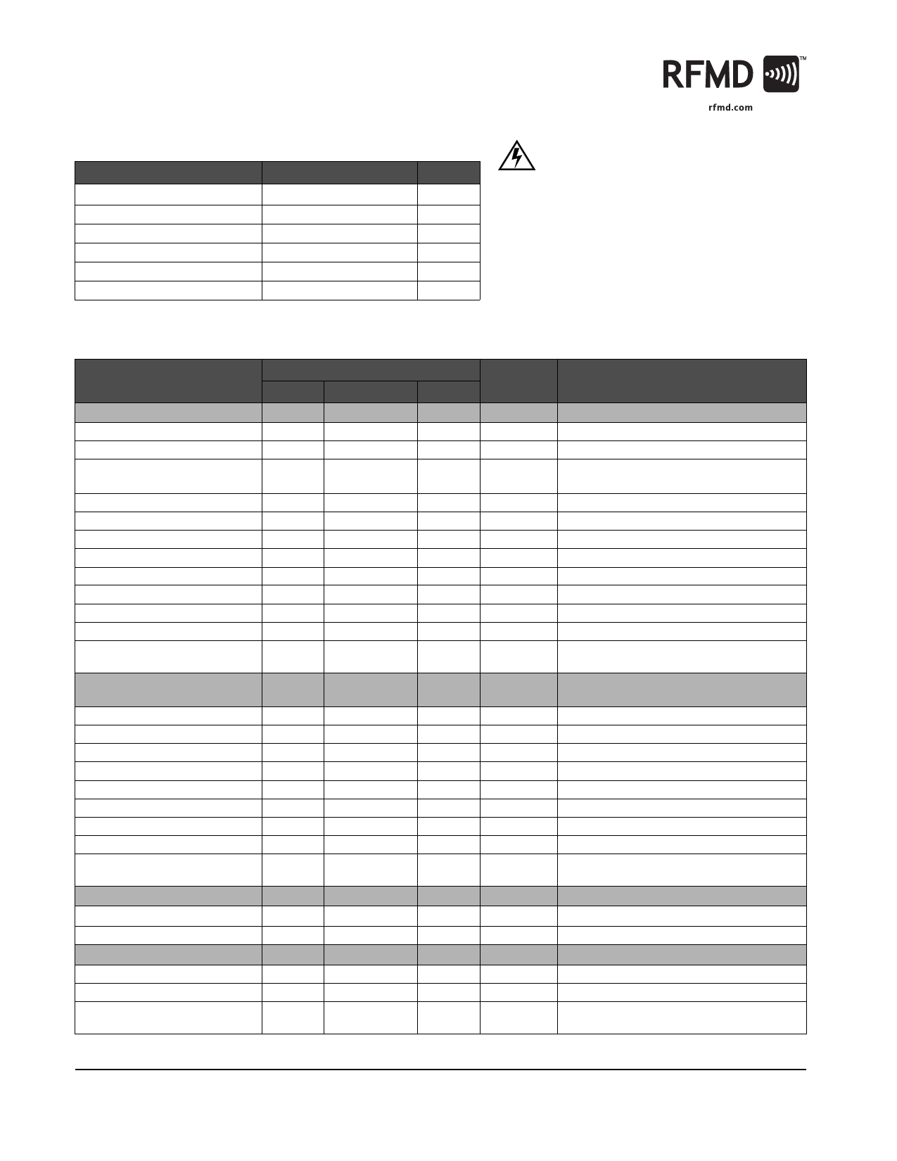
Absolute Maximum Ratings
Parameter
Supply Voltage
Input RF Level
Operating Ambient Temperature
Storage Temperature
Rating
-0.5 to +6.0
+10
-40 to +85
-40 to +150
Unit
VDC
dBm
°C
°C
Caution! ESD sensitive device.
Exceeding any one or a combination of the Absolute Maximum Rating conditions may
cause permanent damage to the device. Extended application of Absolute Maximum
Rating conditions to the device may reduce device reliability. Specified typical perfor-
mance or functional operation of the device under Absolute Maximum Rating condi-
tions is not implied.
RoHS status based on EUDirective2002/95/EC (at time of this document revision).
The information in this publication is believed to be accurate and reliable. However, no
responsibility is assumed by RF Micro Devices, Inc. ("RFMD") for its use, nor for any
infringement of patents, or other rights of third parties, resulting from its use. No
license is granted by implication or otherwise under any patent or patent rights of
RFMD. RFMD reserves the right to change component circuitry, recommended appli-
cation circuitry and specifications at any time without prior notice.
Parameter
Overall
RF Frequency Range
950MHz Performance
Gain
Isolation
Gain Step
Noise Figure
Output IP3
Input P1dB
Reverse Isolation
Input VSWR
Output VSWR
1850MHz Performance
Gain
Isolation
Gain Step
Noise Figure
Output IP3
Input P1dB
Reverse Isolation
Input VSWR
Output VSWR
LNA Select
“Enable” Voltage
“Disable” Voltage
Power Supply
Voltage
Current Consumption
Specification
Min.
Typ.
Max.
800 to 1000
1800 to 2000
16
18
20
16
34
1.3
+17
+24
-10
20
1.8:1
2:1
1.8:1
2:1
20
21.5
24
10
31.5
1.4
+16
+22
-12
30
1.7:1
2:1
1.7:1
2:1
VCC
0
2.8
2.5 to 5.0
5
Unit
Condition
MHz
MHz
T = 25°C, RF=950MHz, VCC=2.8V,
EN1=2.8V, EN2=0V
dB
dB
EN1 = 0 V
dB
Gain - Isolation
dB
dBm
dBm
dB
No external matching
With external match as per GSM/DCS Applica-
tion Schematic
T = 25°C, RF=1850MHz, VCC=2.8V,
EN2=2.8V, EN1=0V
dB
dB
EN2 = 0 V
dB
Gain - Isolation
dB
dBm
dBm
dB
No external matching
With external match as per GSM/DCS Applica-
tion Schematic
V
V
T = 25 °C
V
Specifications
V
Operating limits
mA
900MHz LNA Enabled, 1900MHz LNA Dis-
abled; total DC current
2 of 12
7628 Thorndike Road, Greensboro, NC 27409-9421 · For sales or technical
support, contact RFMD at (+1) 336-678-5570 or sales-support@rfmd.com.
Rev B3 DS040114
Share Link: 