HIP1011D(1999) データシートの表示(PDF) - Intersil
部品番号
コンポーネント説明
一致するリスト
HIP1011D Datasheet PDF : 15 Pages
| |||
HIP1011D
Using the HIP1011DEVAL1 Platform
General and Biasing Information
The HIP1011DEVAL1 platform (Figure 24) comes as a three
part set consisting of 1 mother board emulator and 2 load
cards. This evaluation platform allows a designer to evaluate
and modify the performance and functionality of the
HIP1011D in a simple environment.
Test point numbers (TP#) correspond to the HIP1011D
device (U5) pin numbers thus TP3 and TP12 are PWRON_2
and PWRON_1 respectively. These 2 pins are the HIP1011D
control inputs for each of the 2 integrated but independent
PCI power controllers in the HIP1011D.
On the HIP1011DEVAL1 platform are 4 HUF76132SK8,
(11.5mΩ, 30V, 11.5A) N-Channel power MOSFETs, (Q1-
Q4) these are used as the external switches for the +5V and
+3.3V supplies to the load card connectors, P1 and P2.
Current sensing is facilitated by the four 5mΩ 1W metal strip
resistors (R1-R4), the voltages developed across the sense
resistors are compared to references on board the
HIP1011D.
The HIP1011DEVAL1 platform is powered through the J1 to
J5 connector jacks near the top of the board, see Table 2 for
bias voltage assignments.
TABLE 2. HIP1011DEVAL1 BIAS ASSIGNMENTS
J1
J2
J3
J4
J5
GND
+5V
-12V
+12V
+3.3V
After properly biasing the HIP1011D and ensuring there is
an adequate ground return from the HIP1011DEVAL1
platform to the power supplies, (otherwise anomalous and
unpredictable results will occur) signal the PWRON inputs
low then insert the load cards as shown in Figure 15.
Signaling either or both PWRON pins high (>2.4V) will turn
on the appropriate FET switches and apply voltage to the
load cards.
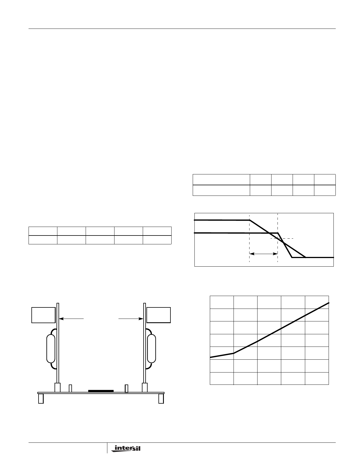
LOAD CARDS
HIP1011D
Evaluating Time Delay to Latch-Off
Provided for delay to latch-off evaluation are 2 locations for
1206 SMD capacitors, C7 and C8. Filling these locations
places a capacitor to ground from each of the HIP1011D
FLTN pins thus tailoring the FLTN signal going low ramp
rate. This provides a delay to the fault signal latch-off
threshold voltage, FLTN Vth. By increasing this time the
HIP1011D delays immediate latch-off of the bus supply
switches, thus ignoring transient OC and UV conditions. See
Table 3 illustrating the time it takes for switch gate turn-off
from the FLTN start of response to an OC or UV condition.
The FLTN response to an OC or UV condition is 110ns. See
Figures 20 through 23 for waveforms.
The intent of any protection device is to isolate the supply
quickly so a faulty card does not drag down a supply. A
longer latch-off delay results in less isolation from a faulty
card to supply.
TABLE 3.
C7 AND C8 VALUE OPEN 0.001µF 0.01µF 0.1µF
FLTN to Gate Response 0.1µs 0.44µs 2.9µs 28µs
FLTN
3V5VG
FLTN, Vth
FIGURE 16. TIMING DIAGRAM
10ms
1ms
100µs
10µs
1µs
100ns
10ns
1ns
OPEN
0.001µF
0.01µF
0.1µF
1µF
10µF
FIGURE 17. TYPICAL OC/UV TO VG RESPONSE vs FLTN CAP
FIGURE 15. cORRECT INSTALLATION OF LOAD CARDS
11
Share Link: 