NCP1217P65G(2010) データシートの表示(PDF) - ON Semiconductor
部品番号
コンポーネント説明
一致するリスト
NCP1217P65G
(Rev.:2010)
(Rev.:2010)
ON Semiconductor

NCP1217P65G Datasheet PDF : 19 Pages
| |||
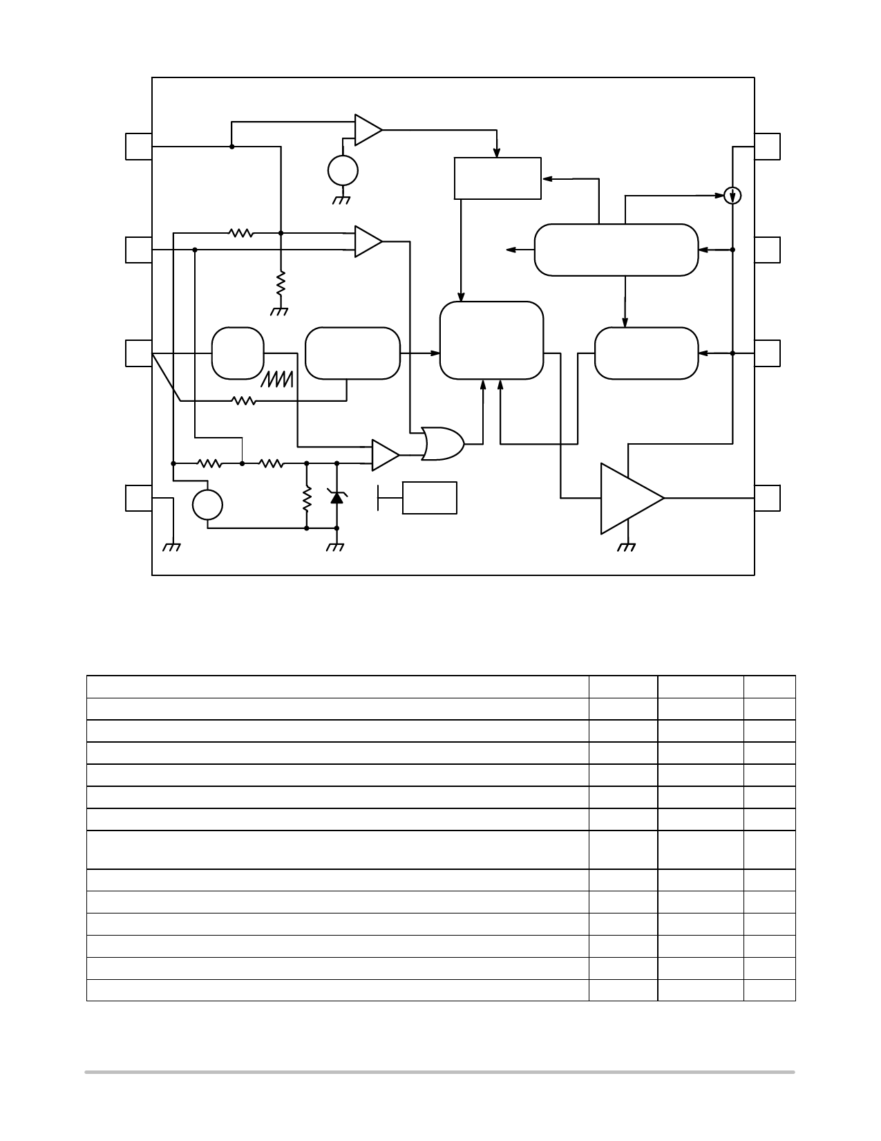
NCP1217, NCP1217A
Adj
1
FB
2
Current
Sense
3
Ground
4
Latchoff
+ Comparator
--
+
-- 3.1 V
Set
Reset
Latch
UVLO
HV
8
HV Current
Source
80 k
1.1 V
Skip Cycle
+ Comparator
NC
--
UVLO High and Low
7
Internal VCC
24 k
Reset
Q Flip--Flop
VCC
250 ns
L.E.B.
65--100--133 kHz Set DCmax = 74% Q
Clock
Reset
Overload
Management
6
19 k
Ramp
Compensation
20 k
57 k
VREF
+
--
25 k
+
--
1V
1ms SS*
Drv
500 mA
5
* Available for “A” version only
Figure 2. Internal Circuit Architecture
MAXIMUM RATINGS
Rating
Symbol
Value
Unit
Power Supply Voltage
Power Supply Voltage on All Other Pins Except Pin 8 (HV), Pin 6 (VCC) and Pin 5 (Drv)
Maximum Voltage on Pin 8 (HV), Pin 6 (VCC) Decoupled to Ground with 10 mF
Maximum Voltage on Pin 8 (HV), Pin 6 (VCC) Grounded
Minimum Operating Voltage on Pin 8 (HV)
VCC
16
V
--
--0.3 to 10
V
VHV
500
V
VHV
450
V
28
V
Maximum Current into All Pins Except VCC (6) and HV (8) when 10 V ESD Diodes are Activated
Thermal Resistance, Junction--to--Case
Thermal Resistance, Junction--to--Air, PDIP--7 Version
Thermal Resistance, Junction--to--Air, SO--8 Version
Maximum Junction Temperature
Temperature Shutdown
Hysteresis in Shutdown
Storage Temperature Range
--
RθJC
RθJA
RθJA
TJMAX
--
--
--
5.0
57
100
178
150
155
30
--60 to +150
mA
C/W
C/W
C
C
C
C
ESD Capability, HBM Model (All Pins Except VCC and HV)
ESD Capability, Machine Model
--
2.0
kV
--
200
V
Stresses exceeding Maximum Ratings may damage the device. Maximum Ratings are stress ratings only. Functional operation above the
Recommended Operating Conditions is not implied. Extended exposure to stresses above the Recommended Operating Conditions may affect
device reliability.
http://onsemi.com
3
Share Link: