TC74LCX02FT データシートの表示(PDF) - Toshiba
部品番号
コンポーネント説明
一致するリスト
TC74LCX02FT Datasheet PDF : 10 Pages
| |||
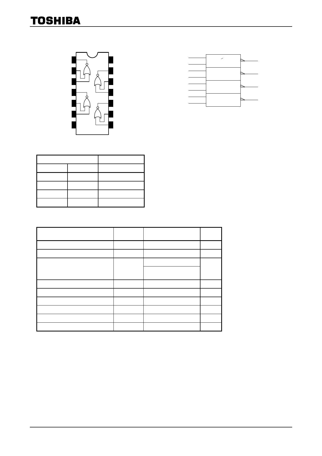
Pin Assignment (top view)
1Y 1
1A 2
1B 3
2Y 4
2A 5
2B 6
GND 7
14 VCC
13 4Y
12 4B
11 4A
10 3Y
9 3B
8 3A
TC74LCX02F/FT/FK
IEC Logic Symbol
1A 2
1B 3
2A 5
2B 6
3A 8
3B 9
4A 11
4B 12
>1
1 1Y
4 2Y
10 3Y
13 4Y
Truth Table
Inputs
A
B
L
L
L
H
H
L
H
H
Outputs
Y
H
L
L
L
Absolute Maximum Ratings (Note 1)
Characteristics
Symbol
Rating
Unit
Power supply voltage
DC input voltage
DC output voltage
Input diode current
Output diode current
DC output current
Power dissipation
DC VCC/ground current
Storage temperature
VCC
VIN
VOUT
IIK
IOK
IOUT
PD
ICC/IGND
Tstg
−0.5 to 7.0
V
−0.5 to 7.0
V
−0.5 to 7.0 (Note 2)
−0.5 to VCC 0.5
V
(Note 3)
−50
mA
±50 (Note 4) mA
±50
mA
180
mW
±100
mA
−65 to 150
°C
Note 1: Exceeding any of the absolute maximum ratings, even briefly, lead to deterioration in IC performance or even
destruction.
Using continuously under heavy loads (e.g. the application of high temperature/current/voltage and the
significant change in temperature, etc.) may cause this product to decrease in the reliability significantly even
if the operating conditions (i.e. operating temperature/current/voltage, etc.) are within the absolute maximum
ratings and the operating ranges.
Please design the appropriate reliability upon reviewing the Toshiba Semiconductor Reliability Handbook
(“Handling Precautions”/“Derating Concept and Methods”) and individual reliability data (i.e. reliability test
report and estimated failure rate, etc).
Note 2: VCC = 0 V
Note 3: High or low state. IOUT absolute maximum rating must be observed.
Note 4: VOUT < GND, VOUT > VCC
2
2014-03-01
Share Link: 