L4937NPD データシートの表示(PDF) - STMicroelectronics
部品番号
コンポーネント説明
一致するリスト
L4937NPD Datasheet PDF : 9 Pages
| |||
L4937NPD
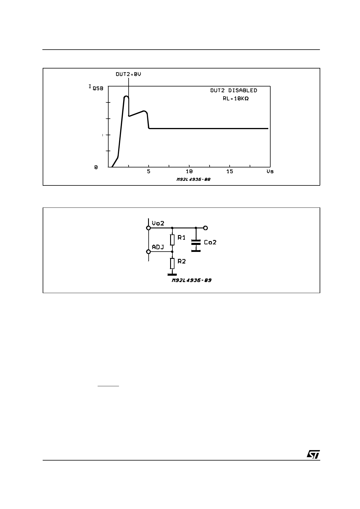
Figure 2 : Quiescent Current vs. Supply Voltage.
400µ
200µ
Figure 3 : Programmable Output 2 Voltage with External Resistors.
RESET CIRCUIT
The block circuit diagram of the reset circuit is shown
in fig. 4. The reset circuit supervises the standby out-
put voltage. The reset threshold of 4.7V is defined
by the internal reference voltage and the standby
output divider.
The reset pulse delay time tRD, is defined by the
charge time of an external capacitor CT :
tRD =
CT x 2V
2µA
The reaction time of the reset circuit depends on the
discharge time limitation of the reset capacitor CT
and is proportional to the value of CT.
The reaction time of the reset circuit increases the
noise immunity. In fact, if the standby output voltage
drops below the reset threshold for a time shorter
than the reaction time tRR, no reset output variation
occurs. The nominal reset delay is generated for
standby output voltage drops longer than the time
necessary for the complete discharging of the ca-
pacitor CT. This time is typically equal to 50µs if
CT = 100nF. The typical reset output waveforms are
shown in fig. 5.
6/9
Share Link: 