W83194BR-S データシートの表示(PDF) - Winbond
部品番号
コンポーネント説明
一致するリスト
W83194BR-S Datasheet PDF : 17 Pages
| |||
W83194BR-S
PRELIMINARY
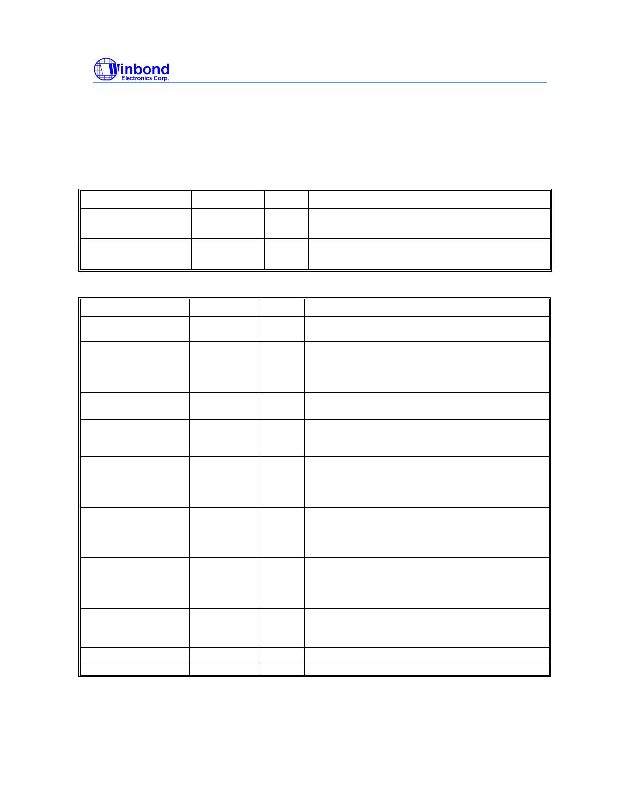
4.1 Crystal I/O
SYMBOL
Xin
Xout
PIN
I/O
FUNCTION
3
IN Crystal input with internal loading capacitors(36pF)
and feedback resistors.
4
OUT Crystal output at 14.318MHz nominally with internal
loading capacitors(36pF).
4.2 CPU, SDRAM, PCI, IOAPIC Clock Outputs
SYMBOL
CPUCLK [0:1]
PD#/RESET$
IOAPIC
SDRAM [ 0:8]
PCICLK0/ *FS0
PCICLK1/ FS1#
PCICLK2/ *FS2
PCICLK3/MODE1*
PCICLK [ 4:6 ]
3V66 [0:2]
PIN
45,44
29
47
41,40,
39,37,36,35,33
,32,31
11
12
13
15
16,18,19
7,8,9
I/O
OUT
IN
OUT
OUT
I/O
I/O
I/O
I/O
OUT
OUT
FUNCTION
Low skew (< 250ps) clock outputs for host
frequencies such as CPU and Chipset.
Pin16 *Mode1=1, Power Down mode when driven
low.
Pin16 *Mode1=0, RESET# output (4ms low active
pulse when Watch Dog time out)
Clock outputs synchronous with PCI clock and
powered by VddA.
SDRAM clock outputs.
3.3V 33MHz PCI clock during normal operation.
Latched input for FS0 at initial power up for H/W
selecting the output frequency of CPU, SDRAM and
PCI clocks(Default=1).
Low skew (< 250ps) PCI clock outputs.
Latched input for FS1 at initial power up for H/W
selecting the output frequency of CPU, SDRAM and
PCI clocks(Default=0).
Low skew (< 250ps) PCI clock outputs.
Latched input for FS2 at initial power up for H/W
selecting the output frequency of CPU, SDRAM and
PCI clocks(Default=1).
PCI clock during normal operation.
Latched Input. *Mode1=1, Pin 29 is PD#; *Mode1=0,
Pin 29 is RESET$
Low skew (< 250ps) PCI clock outputs.
3.3V output clocks for the chipset.
-3-
Publication Release Date: June 2000
Revision
0.42
Share Link: 